- 您现在的位置:买卖IC网 > PDF目录10803 > AD5318BRU-REEL7 (Analog Devices Inc)IC DAC 10BIT OCTAL BUFF 16-TSSOP PDF资料下载
参数资料
| 型号: | AD5318BRU-REEL7 |
| 厂商: | Analog Devices Inc |
| 文件页数: | 10/28页 |
| 文件大小: | 0K |
| 描述: | IC DAC 10BIT OCTAL BUFF 16-TSSOP |
| 产品培训模块: | Data Converter Fundamentals DAC Architectures |
| 产品变化通告: | Product Discontinuance 27/Oct/2011 |
| 标准包装: | 1,000 |
| 设置时间: | 6µs |
| 位数: | 10 |
| 数据接口: | 串行 |
| 转换器数目: | 8 |
| 电压电源: | 单电源 |
| 功率耗散(最大): | 4.5mW |
| 工作温度: | -40°C ~ 105°C |
| 安装类型: | 表面贴装 |
| 封装/外壳: | 16-TSSOP(0.173",4.40mm 宽) |
| 供应商设备封装: | 16-TSSOP |
| 包装: | 带卷 (TR) |
| 输出数目和类型: | 8 电压,单极;8 电压,双极 |
| 采样率(每秒): | 167k |
第1页第2页第3页第4页第5页第6页第7页第8页第9页当前第10页第11页第12页第13页第14页第15页第16页第17页第18页第19页第20页第21页第22页第23页第24页第25页第26页第27页第28页
AD5308/AD5318/AD5328
Rev. F | Page 18 of 28
Power-Down Mode
The individual channels of the AD5308/AD5318/AD5328 can
be powered down separately. The control mode for this is (10).
On completion of this write sequence, the channels that have
been set to 1 are powered down.
Reset Mode
This mode consists of two possible reset functions, as outlined
in Table 9.
Table 9. Reset Mode
Bit 15
Bit 14
Bit 13
Bit 12
Bit 11 ... 0
Description
1
0
x ... x
DAC data reset
1
x ... x
Data and control reset
DAC Data Reset: On completion of this write sequence, all
DAC registers and input registers are filled with 0s.
Data and Control Reset: This function carries out a DAC data
reset and resets all the control bits (GAIN, BUF, VDD, LDAC, and
power-down channels) to their power-on conditions.
LOW POWER SERIAL INTERFACE
To minimize the power consumption of the device, the interface
powers up fully only when the device is being written to, that is,
on the falling edge of SYNC. The SCLK and DIN input buffers
are powered down on the rising edge of SYNC.
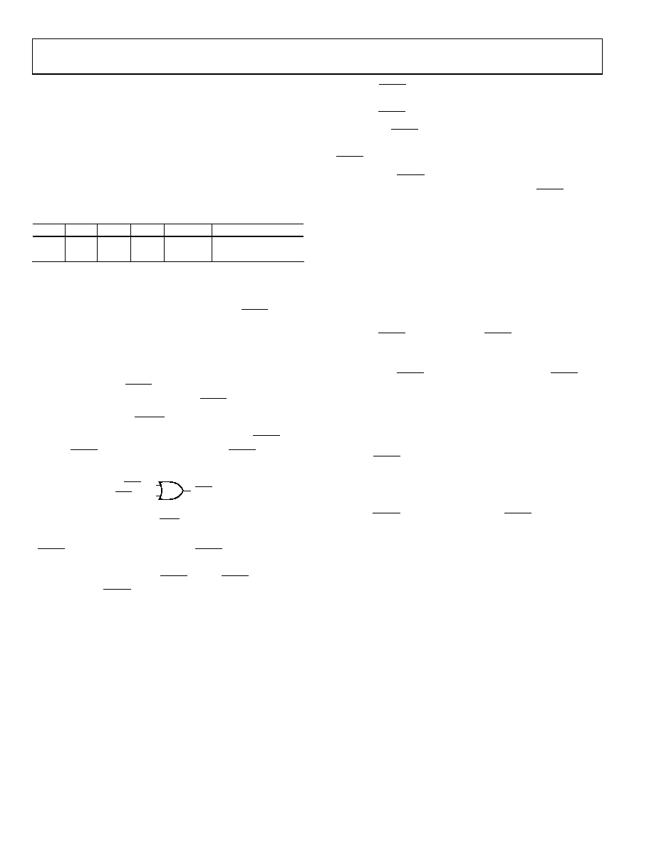
LOAD DAC INPUT (LDAC) FUNCTION
Access to the DAC registers is controlled by both the LDAC pin
and the LDAC mode bits. The operation of the LDAC function
can be likened to the configuration shown in
02812-034
LDAC FUNCTION
EXTERNAL LDAC PIN
INTERNAL LDAC MODE
Figure 35. LDAC Function
If the user wishes to update the DAC through software, the
LDAC pin should be tied high and the LDAC mode bits set as
required. Alternatively, if the user wishes to control the DAC
through hardware, that is, the LDAC pin, the LDAC mode bits
should be set to LDAC high (default mode).
Use of the LDAC function enables double-buffering of the DAC
data, and the GAIN, BUF and VDD bits. There are two ways in
which the LDAC function can operate:
Synchronous LDAC: The DAC registers are updated after new
data is read in on the falling edge of the 16th SCLK pulse.
LDAC can be permanently low or pulsed as in
.
Asynchronous LDAC: The outputs are not updated at the same
time that the input registers are written to. When LDAC goes
low, the DAC registers are updated with the contents of the
input register.
DOUBLE-BUFFERED INTERFACE
The AD5308/AD5318/AD5328 DACs all have double-buffered
interfaces consisting of two banks of registers: input and DAC.
The input registers are connected directly to the input shift
register and the digital code is transferred to the relevant input
register on completion of a valid write sequence. The DAC
registers contain the digital code used by the resistor strings.
When the LDAC pin is high and the LDAC bits are set to (01),
the DAC registers are latched and the input registers can change
state without affecting the contents of the DAC registers. How-
ever, when the LDAC bits are set to (00) or when the LDAC pin
is brought low, the DAC registers become transparent and the
contents of the input registers are transferred to them.
The double-buffered interface is useful if the user requires
simultaneous updating of all DAC outputs. The user can write
up to seven of the input registers individually and then, by
bringing LDAC low when writing to the remaining DAC input
register, all outputs will update simultaneously.
These parts contain an extra feature whereby a DAC register is
not updated unless its input register has been updated since the
last time LDAC was low. Normally, when LDAC is brought low,
the DAC registers are filled with the contents of the input regis-
ters. In the case of the AD5308/AD5318/AD5328, the part
updates the DAC register only if the input register has been
changed since the last time the DAC register was updated,
thereby removing unnecessary digital crosstalk.
相关PDF资料 |
PDF描述 |
|---|---|
| AD5317BRU-REEL | IC DAC 10BIT QUAD W/BUFF 16TSSOP |
| AD5316BRU-REEL7 | IC DAC 10BIT QUAD W/BUFF 16TSSOP |
| BU7251G-TR | IC COMPARATOR SGL 5.5V SSOP-5 |
| AD5301BRM-REEL7 | IC DAC 8BIT 2WIRE I2C 8-MSOP |
| ADM238LARZ | IC TXRX RS-232 4:4 5V LP 24SOIC |
相关代理商/技术参数 |
参数描述 |
|---|---|
| AD5318BRUZ | 功能描述:IC DAC 10BIT OCTAL W/BUF 16TSSOP RoHS:是 类别:集成电路 (IC) >> 数据采集 - 数模转换器 系列:- 产品培训模块:Lead (SnPb) Finish for COTS Obsolescence Mitigation Program 标准包装:50 系列:- 设置时间:4µs 位数:12 数据接口:串行 转换器数目:2 电压电源:单电源 功率耗散(最大):- 工作温度:-40°C ~ 85°C 安装类型:表面贴装 封装/外壳:8-TSSOP,8-MSOP(0.118",3.00mm 宽) 供应商设备封装:8-uMAX 包装:管件 输出数目和类型:2 电压,单极 采样率(每秒):* 产品目录页面:1398 (CN2011-ZH PDF) |
| AD5318BRUZ-REEL | 功能描述:IC DAC 10BIT OCTAL W/BUF 16TSSOP RoHS:是 类别:集成电路 (IC) >> 数据采集 - 数模转换器 系列:- 标准包装:47 系列:- 设置时间:2µs 位数:14 数据接口:并联 转换器数目:1 电压电源:单电源 功率耗散(最大):55µW 工作温度:-40°C ~ 85°C 安装类型:表面贴装 封装/外壳:28-SSOP(0.209",5.30mm 宽) 供应商设备封装:28-SSOP 包装:管件 输出数目和类型:1 电流,单极;1 电流,双极 采样率(每秒):* |
| AD5318BRUZ-REEL7 | 功能描述:IC DAC 10BIT OCTAL W/BUF 16TSSOP RoHS:是 类别:集成电路 (IC) >> 数据采集 - 数模转换器 系列:- 标准包装:47 系列:- 设置时间:2µs 位数:14 数据接口:并联 转换器数目:1 电压电源:单电源 功率耗散(最大):55µW 工作温度:-40°C ~ 85°C 安装类型:表面贴装 封装/外壳:28-SSOP(0.209",5.30mm 宽) 供应商设备封装:28-SSOP 包装:管件 输出数目和类型:1 电流,单极;1 电流,双极 采样率(每秒):* |
| AD532 | 制造商:未知厂家 制造商全称:未知厂家 功能描述:Internally Trimmed Integrated Circuit Multiplier |
| AD5320 | 制造商:AD 制造商全称:Analog Devices 功能描述:2.5 V to 5.5 V, 500 uA, Parallel Interface Quad Voltage-Output 8-/10-/12-Bit DACs |
发布紧急采购,3分钟左右您将得到回复。