- 您现在的位置:买卖IC网 > PDF目录10803 > AD5318BRU-REEL7 (Analog Devices Inc)IC DAC 10BIT OCTAL BUFF 16-TSSOP PDF资料下载
参数资料
| 型号: | AD5318BRU-REEL7 |
| 厂商: | Analog Devices Inc |
| 文件页数: | 8/28页 |
| 文件大小: | 0K |
| 描述: | IC DAC 10BIT OCTAL BUFF 16-TSSOP |
| 产品培训模块: | Data Converter Fundamentals DAC Architectures |
| 产品变化通告: | Product Discontinuance 27/Oct/2011 |
| 标准包装: | 1,000 |
| 设置时间: | 6µs |
| 位数: | 10 |
| 数据接口: | 串行 |
| 转换器数目: | 8 |
| 电压电源: | 单电源 |
| 功率耗散(最大): | 4.5mW |
| 工作温度: | -40°C ~ 105°C |
| 安装类型: | 表面贴装 |
| 封装/外壳: | 16-TSSOP(0.173",4.40mm 宽) |
| 供应商设备封装: | 16-TSSOP |
| 包装: | 带卷 (TR) |
| 输出数目和类型: | 8 电压,单极;8 电压,双极 |
| 采样率(每秒): | 167k |
第1页第2页第3页第4页第5页第6页第7页当前第8页第9页第10页第11页第12页第13页第14页第15页第16页第17页第18页第19页第20页第21页第22页第23页第24页第25页第26页第27页第28页
AD5308/AD5318/AD5328
Rev. F | Page 16 of 28
POWER-ON RESET
The AD5308/AD5318/AD5328 are provided with a power-on
reset function so that they power up in a defined state. The
power-on state is
Normal operation
Reference inputs unbuffered
0 V to VREF output range
Output voltage set to 0 V
LDAC bits set to LDAC high
Both input and DAC registers are filled with 0s and remain so
until a valid write sequence is made to the device. This is
particularly useful in applications where it is important to know
the state of the DAC outputs while the device is powering up.
POWER-DOWN MODE
The AD5308/AD5318/AD5328 have low power consumption,
typically dissipating 2.4 mW with a 3 V supply and 5 mW with
a 5 V supply. Power consumption can be further reduced when
the DACs are not in use by putting them into power-down
mode, which is described in the Serial Interface section.
When in default mode, all DACs work normally with a typical
power consumption of 1 mA at 5 V (800 μA at 3 V). However,
when all DACs are powered down, that is, in power-down
mode, the supply current falls to 400 nA at 5 V (120 nA at 3 V).
Not only does the supply current drop, but the output stage is
also internally switched from the output of the amplifier,
making it open-circuit. This has the advantage that the output is
three-state while the part is in power-down mode, and provides
a defined input condition for whatever is connected to the
output of the DAC amplifier. The output stage is illustrated in
The bias generator, the output amplifiers, the resistor string, and
all other associated linear circuitry are shut down when the
power-down mode is activated. However, the contents of the
registers are unaffected when in power-down. In fact, it is
possible to load new data to the input registers and DAC regis-
ters during power-down. The DAC outputs update as soon as
the device comes out of power-down mode. The time to exit
power-down is typically 2.5 μs when VDD = 5 V and 5 μs when
VDD = 3 V.
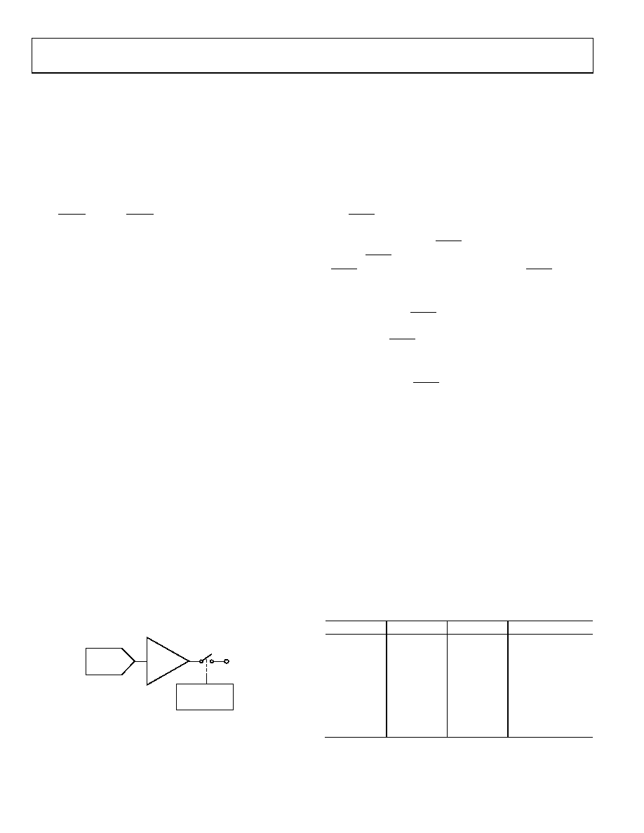
02812-035
POWER-DOWN
CIRCUITRY
RESISTOR-
STRING DAC
AMPLIFIER
VOUT
Figure 31. Output Stage During Power-Down
SERIAL INTERFACE
The AD5308/AD5318/AD5328 are controlled over a versatile
3-wire serial interface that operates at clock rates up to 30 MHz
and is compatible with SPI, QSPI, MICROWIRE, and DSP
interface standards.
Input Shift Register
The input shift register is 16 bits wide. Data is loaded into the
device as a 16-bit word under the control of a serial clock input,
SCLK. The timing diagram for this operation is shown in Figure 2.
The SYNC input is a level-triggered input that acts as a frame
synchronization signal and chip enable. Data can be transferred
into the device only while SYNC is low. To start the serial data
transfer, SYNC should be taken low, observing the minimum
SYNC to SCLK falling edge set-up time, t4. After SYNC goes
low, serial data is shifted into the device’s input shift register on
the falling edges of SCLK for 16 clock pulses.
To end the transfer, SYNC must be taken high after the falling
edge of the 16th SCLK pulse, observing the minimum SCLK
falling edge to SYNC rising edge time, t7.
After the end of the serial data transfer, data is automatically
transferred from the input shift register to the input register of
the selected DAC. If SYNC is taken high before the 16th falling
edge of SCLK, the data transfer is aborted and the DAC input
registers are not updated.
Data is loaded MSB first (Bit 15). The first bit determines
whether it is a DAC write or a control function.
DAC Write
The 16-bit word consists of 1 control bit and 3 address bits fol-
lowed by 8, 10, or 12 bits of DAC data, depending on the device
type. In the case of a DAC write, the MSB is a 0. The next 3
address bits determine whether the data is for DAC A, DAC B,
DAC C, DAC D, DAC E, DAC F, DAC G, or DAC H. The
AD5328 uses all 12 bits of DAC data. The AD5318 uses 10 bits
and ignores the 2 LSBs. The AD5308 uses 8 bits and ignores the
last 4 bits. These ignored LSBs should be set to 0. The data
format is straight binary, with all 0s corresponding to 0 V
output and all 1s corresponding to full-scale output.
Table 6. Address Bits for the AD5308/AD5318/AD5328
A2 (Bit 14)
A1 (Bit 13)
A0 (Bit 12)
DAC Addressed
0
DAC A
0
1
DAC B
0
1
0
DAC C
0
1
DAC D
1
0
DAC E
1
0
1
DAC F
1
0
DAC G
1
DAC H
相关PDF资料 |
PDF描述 |
|---|---|
| AD5317BRU-REEL | IC DAC 10BIT QUAD W/BUFF 16TSSOP |
| AD5316BRU-REEL7 | IC DAC 10BIT QUAD W/BUFF 16TSSOP |
| BU7251G-TR | IC COMPARATOR SGL 5.5V SSOP-5 |
| AD5301BRM-REEL7 | IC DAC 8BIT 2WIRE I2C 8-MSOP |
| ADM238LARZ | IC TXRX RS-232 4:4 5V LP 24SOIC |
相关代理商/技术参数 |
参数描述 |
|---|---|
| AD5318BRUZ | 功能描述:IC DAC 10BIT OCTAL W/BUF 16TSSOP RoHS:是 类别:集成电路 (IC) >> 数据采集 - 数模转换器 系列:- 产品培训模块:Lead (SnPb) Finish for COTS Obsolescence Mitigation Program 标准包装:50 系列:- 设置时间:4µs 位数:12 数据接口:串行 转换器数目:2 电压电源:单电源 功率耗散(最大):- 工作温度:-40°C ~ 85°C 安装类型:表面贴装 封装/外壳:8-TSSOP,8-MSOP(0.118",3.00mm 宽) 供应商设备封装:8-uMAX 包装:管件 输出数目和类型:2 电压,单极 采样率(每秒):* 产品目录页面:1398 (CN2011-ZH PDF) |
| AD5318BRUZ-REEL | 功能描述:IC DAC 10BIT OCTAL W/BUF 16TSSOP RoHS:是 类别:集成电路 (IC) >> 数据采集 - 数模转换器 系列:- 标准包装:47 系列:- 设置时间:2µs 位数:14 数据接口:并联 转换器数目:1 电压电源:单电源 功率耗散(最大):55µW 工作温度:-40°C ~ 85°C 安装类型:表面贴装 封装/外壳:28-SSOP(0.209",5.30mm 宽) 供应商设备封装:28-SSOP 包装:管件 输出数目和类型:1 电流,单极;1 电流,双极 采样率(每秒):* |
| AD5318BRUZ-REEL7 | 功能描述:IC DAC 10BIT OCTAL W/BUF 16TSSOP RoHS:是 类别:集成电路 (IC) >> 数据采集 - 数模转换器 系列:- 标准包装:47 系列:- 设置时间:2µs 位数:14 数据接口:并联 转换器数目:1 电压电源:单电源 功率耗散(最大):55µW 工作温度:-40°C ~ 85°C 安装类型:表面贴装 封装/外壳:28-SSOP(0.209",5.30mm 宽) 供应商设备封装:28-SSOP 包装:管件 输出数目和类型:1 电流,单极;1 电流,双极 采样率(每秒):* |
| AD532 | 制造商:未知厂家 制造商全称:未知厂家 功能描述:Internally Trimmed Integrated Circuit Multiplier |
| AD5320 | 制造商:AD 制造商全称:Analog Devices 功能描述:2.5 V to 5.5 V, 500 uA, Parallel Interface Quad Voltage-Output 8-/10-/12-Bit DACs |
发布紧急采购,3分钟左右您将得到回复。