- 您现在的位置:买卖IC网 > PDF目录10803 > AD5318BRU-REEL7 (Analog Devices Inc)IC DAC 10BIT OCTAL BUFF 16-TSSOP PDF资料下载
参数资料
| 型号: | AD5318BRU-REEL7 |
| 厂商: | Analog Devices Inc |
| 文件页数: | 14/28页 |
| 文件大小: | 0K |
| 描述: | IC DAC 10BIT OCTAL BUFF 16-TSSOP |
| 产品培训模块: | Data Converter Fundamentals DAC Architectures |
| 产品变化通告: | Product Discontinuance 27/Oct/2011 |
| 标准包装: | 1,000 |
| 设置时间: | 6µs |
| 位数: | 10 |
| 数据接口: | 串行 |
| 转换器数目: | 8 |
| 电压电源: | 单电源 |
| 功率耗散(最大): | 4.5mW |
| 工作温度: | -40°C ~ 105°C |
| 安装类型: | 表面贴装 |
| 封装/外壳: | 16-TSSOP(0.173",4.40mm 宽) |
| 供应商设备封装: | 16-TSSOP |
| 包装: | 带卷 (TR) |
| 输出数目和类型: | 8 电压,单极;8 电压,双极 |
| 采样率(每秒): | 167k |
第1页第2页第3页第4页第5页第6页第7页第8页第9页第10页第11页第12页第13页当前第14页第15页第16页第17页第18页第19页第20页第21页第22页第23页第24页第25页第26页第27页第28页
AD5308/AD5318/AD5328
Rev. F | Page 21 of 28
APPLICATIONS INFORMATION
TYPICAL APPLICATION CIRCUIT
The AD5308/AD5318/AD5328 can be used with a wide range
of reference voltages where the devices offer full, one-quadrant
multiplying capability over a reference range of 0.25 V to VDD.
More typically, these devices are used with a fixed, precision
reference voltage. Suitable references for 5 V operation are the
AD780, ADR381, and REF192 (2.5 V references). For 2.5 V
operation, a suitable external reference is the AD589 or the
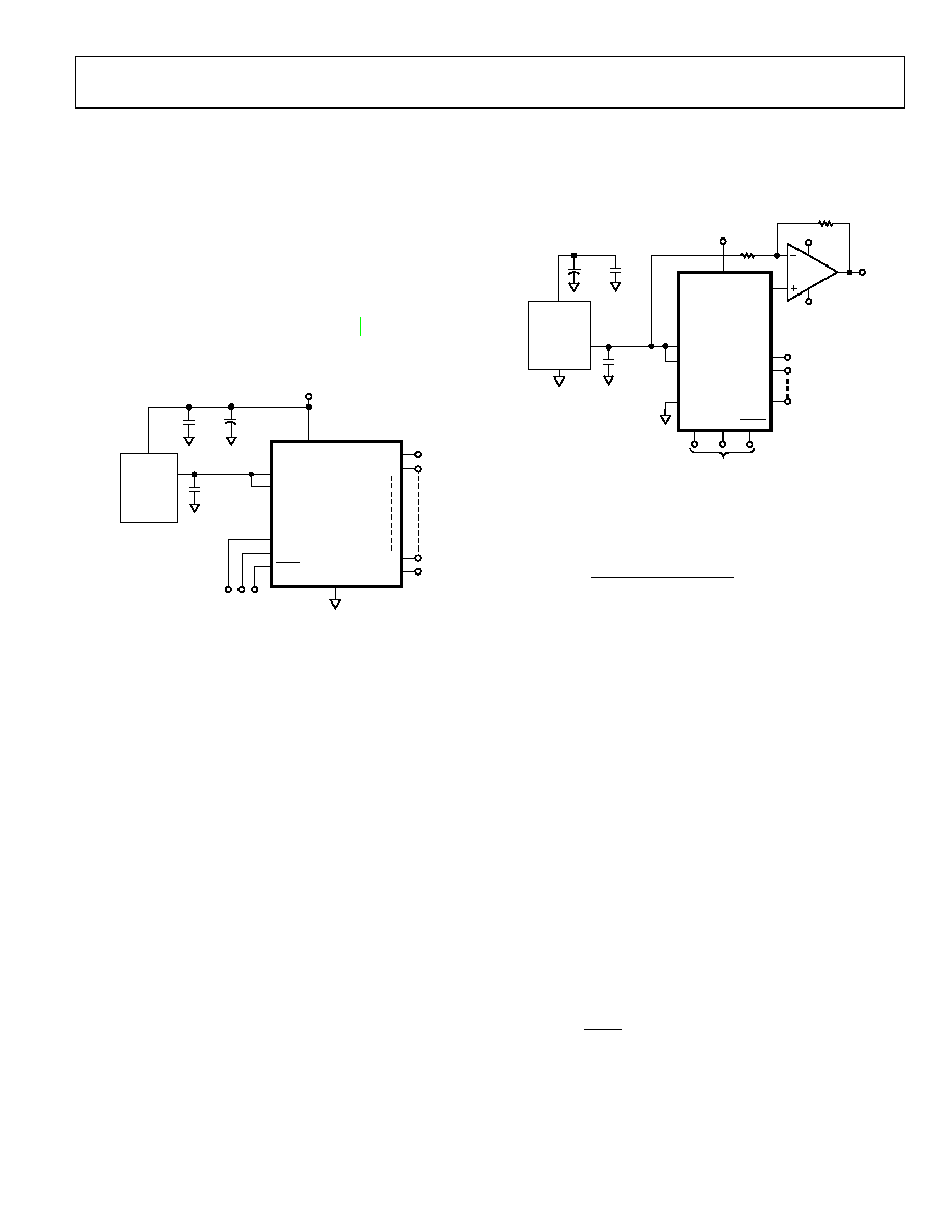
AD1580 (1.2 V band gap references). Figure 40 shows a typical
setup for the AD5308/AD5318/AD5328 when using an external
reference.
02812-040
AD5308/AD5318/
AD5328
GND
DIN
SYNC
SERIAL
INTERFACE
VOUT
EXT
REF
0.1
μF
VREFABCD
VREFEFGH
AD780/ADR3811/REF192
WITH VDD = 5V OR
AD589/AD1580 WITH
VDD = 2.5V
VDD = 2.5V TO 5.5V
VIN
10
μF
1
μF
SCL
VOUTA
VOUTG
VOUTB
VOUTH
Figure 40. AD5308/AD5318/AD5328 Using a 2.5 V or 5 V External Reference
DRIVING VDD FROM THE REFERENCE VOLTAGE
If an output range of 0 V to VDD is required when the reference
inputs are configured as unbuffered, the simplest solution is to
connect the reference input to VDD. As this supply can be noisy
and not very accurate, the AD5308/AD5318/AD5328 can be
powered from a voltage reference. For example, using a 5 V
reference, such as the REF195, works because the REF195
outputs a steady supply voltage for the AD5308/AD5318/
AD5328. The typical current required from the REF195 is a
1 μA supply current and ≈ 112 μA into the reference inputs (if
unbuffered); this is with no load on the DAC outputs. When the
DAC outputs are loaded, the REF195 also needs to supply the
current to the loads. The total current required (with a10 kΩ
load on each output) is
1.22 mA + 8(5 V/10 kΩ) = 5.22 mA
The load regulation of the REF195 is typically 2.0 ppm/mA,
which results in an error of 10.4 ppm (52 μV) for the 5.22 mA
current drawn from it. This corresponds to a 0.003 LSB error at
8 bits and 0.043 LSB error at 12 bits.
BIPOLAR OPERATION USING THE
AD5308/AD5318/AD5328
The AD5308/AD5318/AD5328 have been designed for single-
supply operation, but a bipolar output range is also possible
using the circuit in Figure 41. This circuit gives an output
voltage range of ±5 V. Rail-to-rail operation at the amplifier
output is achievable using an AD820, the AD8519, or an OP196
as the output amplifier.
02812-041
+5V
–5V
AD820/
AD8519/
OP196
10
μF
+6V TO +16V
0.1
μF
R1
10k
Ω
±5V
R2
10k
Ω
GND
VOUT
REF192
+5V
SERIAL
INTERFACE
SCLK SYNC
DIN
1
μF
AD5308/
AD5318/
AD5328
VREFABCD
VREFB
VOUTC
VOUTB
VOUTA
VOUTH
VIN
VDD
Figure 41. Bipolar Operation with the AD5308/AD5318/AD5328
The output voltage for any input code can be calculated as
follows:
(
) ()
()
R1
R
REFIN
R1
R
R1
D
REFIN
V
N
OUT
/
2
/
×
+
×
=
where:
D
is the decimal equivalent of the code loaded to the DAC.
N
is the DAC resolution.
REFIN
is the reference voltage input.
with
REFIN = 5 V , R1 = R2 = 10 kΩ
(
) V
D
V
N
OUT
5
2
/
10
×
=
OPTO-ISOLATED INTERFACE FOR PROCESS
CONTROL APPLICATIONS
The AD5308/AD5318/AD5328 have a versatile 3-wire serial
interface, making them ideal for generating accurate voltages in
process control and industrial applications. Due to noise and
safety requirements, or distance, it may be necessary to isolate
the AD5308/AD5318/AD5328 from the controller. This can
easily be achieved by using opto-isolators that provide isolation
in excess of 3 kV. The actual data rate achieved may be limited
by the type of optocouplers chosen. The serial loading structure
of the AD5308/AD5318/AD5328 makes them ideally suited for
use in opto-isolated applications. Figure 42 shows an opto-
isolated interface to the AD5308/AD5318/AD5328 where DIN,
SCLK, and SYNC are driven from optocouplers. The power
supply to the part also needs to be isolated. This is done by
using a transformer. On the DAC side of the transformer, a 5 V
regulator provides the 5 V supply required for the AD5308/
AD5318/AD5328.
相关PDF资料 |
PDF描述 |
|---|---|
| AD5317BRU-REEL | IC DAC 10BIT QUAD W/BUFF 16TSSOP |
| AD5316BRU-REEL7 | IC DAC 10BIT QUAD W/BUFF 16TSSOP |
| BU7251G-TR | IC COMPARATOR SGL 5.5V SSOP-5 |
| AD5301BRM-REEL7 | IC DAC 8BIT 2WIRE I2C 8-MSOP |
| ADM238LARZ | IC TXRX RS-232 4:4 5V LP 24SOIC |
相关代理商/技术参数 |
参数描述 |
|---|---|
| AD5318BRUZ | 功能描述:IC DAC 10BIT OCTAL W/BUF 16TSSOP RoHS:是 类别:集成电路 (IC) >> 数据采集 - 数模转换器 系列:- 产品培训模块:Lead (SnPb) Finish for COTS Obsolescence Mitigation Program 标准包装:50 系列:- 设置时间:4µs 位数:12 数据接口:串行 转换器数目:2 电压电源:单电源 功率耗散(最大):- 工作温度:-40°C ~ 85°C 安装类型:表面贴装 封装/外壳:8-TSSOP,8-MSOP(0.118",3.00mm 宽) 供应商设备封装:8-uMAX 包装:管件 输出数目和类型:2 电压,单极 采样率(每秒):* 产品目录页面:1398 (CN2011-ZH PDF) |
| AD5318BRUZ-REEL | 功能描述:IC DAC 10BIT OCTAL W/BUF 16TSSOP RoHS:是 类别:集成电路 (IC) >> 数据采集 - 数模转换器 系列:- 标准包装:47 系列:- 设置时间:2µs 位数:14 数据接口:并联 转换器数目:1 电压电源:单电源 功率耗散(最大):55µW 工作温度:-40°C ~ 85°C 安装类型:表面贴装 封装/外壳:28-SSOP(0.209",5.30mm 宽) 供应商设备封装:28-SSOP 包装:管件 输出数目和类型:1 电流,单极;1 电流,双极 采样率(每秒):* |
| AD5318BRUZ-REEL7 | 功能描述:IC DAC 10BIT OCTAL W/BUF 16TSSOP RoHS:是 类别:集成电路 (IC) >> 数据采集 - 数模转换器 系列:- 标准包装:47 系列:- 设置时间:2µs 位数:14 数据接口:并联 转换器数目:1 电压电源:单电源 功率耗散(最大):55µW 工作温度:-40°C ~ 85°C 安装类型:表面贴装 封装/外壳:28-SSOP(0.209",5.30mm 宽) 供应商设备封装:28-SSOP 包装:管件 输出数目和类型:1 电流,单极;1 电流,双极 采样率(每秒):* |
| AD532 | 制造商:未知厂家 制造商全称:未知厂家 功能描述:Internally Trimmed Integrated Circuit Multiplier |
| AD5320 | 制造商:AD 制造商全称:Analog Devices 功能描述:2.5 V to 5.5 V, 500 uA, Parallel Interface Quad Voltage-Output 8-/10-/12-Bit DACs |
发布紧急采购,3分钟左右您将得到回复。