- 您现在的位置:买卖IC网 > PDF目录373878 > AD5338BRMZ-1REEL7 (ANALOG DEVICES INC) 2.5 V to 5.5 V, 250 UA, 2-Wire Interface Dual-Voltage Output, 8-/10-/12-Bit DACs PDF资料下载
参数资料
| 型号: | AD5338BRMZ-1REEL7 |
| 厂商: | ANALOG DEVICES INC |
| 元件分类: | DAC |
| 英文描述: | 2.5 V to 5.5 V, 250 UA, 2-Wire Interface Dual-Voltage Output, 8-/10-/12-Bit DACs |
| 中文描述: | SERIAL INPUT LOADING, 7 us SETTLING TIME, 10-BIT DAC, PDSO8 |
| 封装: | ROHS COMPLIANT, MO-187AA, MSOP-8 |
| 文件页数: | 19/24页 |
| 文件大小: | 654K |
| 代理商: | AD5338BRMZ-1REEL7 |
AD5337/AD5338/AD5339
DOUBLE-BUFFERED INTERFACE
The AD5337/AD5338/AD5339 DACs all have a double-buffered
interface consisting of two banks of registers—an input register
and a DAC register per channel. The input register is directly
connected to the input shift register, and the digital code is
transferred to the relevant input register upon completion of a
valid write sequence. The DAC register contains the digital code
used by the resistor string.
Rev. A | Page 19 of 24
Access to the DAC register is controlled by the LDAC bit. When
the LDAC bit is set high, the DAC register is latched and therefore
the input register may change state without affecting the DAC
register. This is useful if the user requires simultaneous updating
of all DAC outputs. The user may write to three of the input
registers individually; by setting the LDAC bit low when writing
to the remaining DAC input register, all outputs will update
simultaneously.
These parts contain an extra feature whereby the DAC register
is only updated if its input register has been updated since the
last time that LDAC was brought low, thereby removing
unnecessary digital crosstalk.
POWER-DOWN MODES
The AD5337/AD5338/AD5339 have very low power
consumption, typically dissipating 0.75 mW with a 3 V supply
and 1.5 mW with a 5 V supply. Power consumption can be
further reduced when the DACs are not in use by putting them
into one of three power-down modes, which are selected by
Bits 15 and 14 (PD1 and PD0) of the data byte. Table 8 shows
how the state of the bits corresponds to the mode of operation
of the DAC.
Table 8. PD1/PD0 Operating Modes
PD1
PD0
Operating Mode
0
0
Normal Operation
0
1
Power-Down (1 k Load to GND)
1
0
Power-Down (100 k Load to GND)
1
1
Power-Down (3-State Output)
When both bits are 0, the DAC works with its normal power
consumption of 300 μA at 5 V. However, for the three power-
down modes, the supply current falls to 200 nA at 5 V (80 nA at
3 V). Not only does the supply current drop, but the output
stage is also internally switched from the output of the amplifier
to a resistor network of known values. This is advantageous in
that the output impedance of the part is known while the part is
in power-down mode, which provides a defined input condition
for whatever is connected to the output of the DAC amplifier.
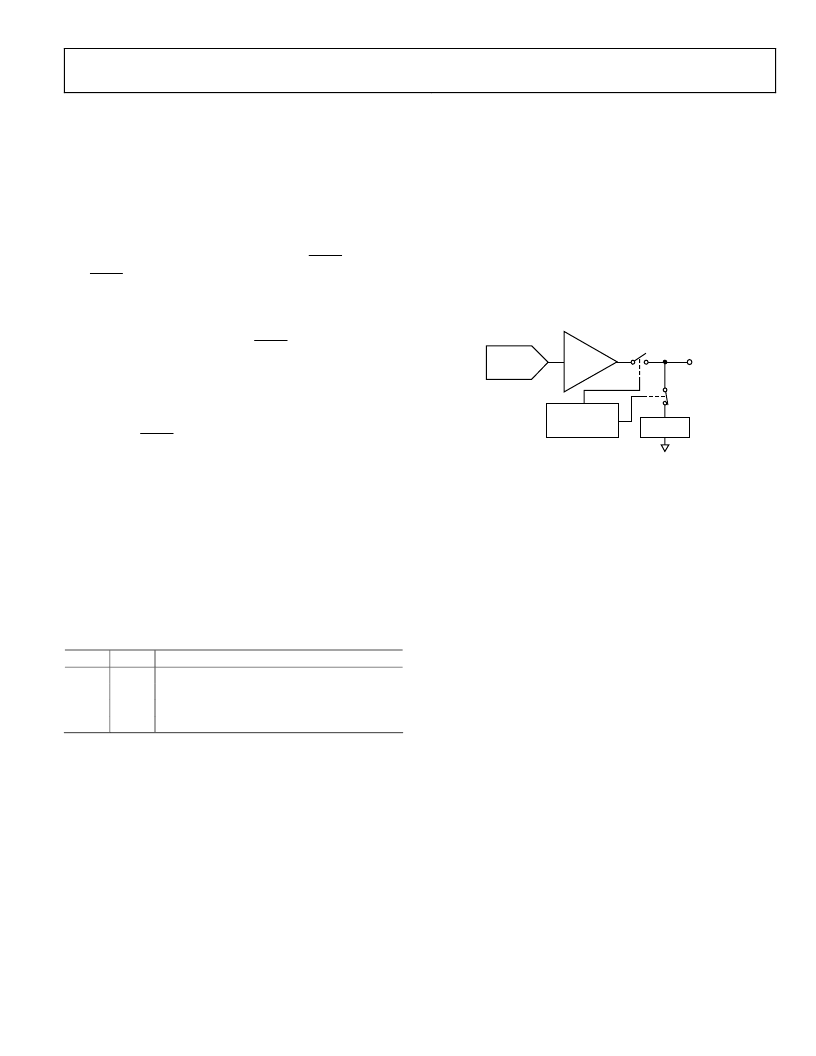
There are three options. The output may be connected internally
to GND through a 1 k resistor, a 100 k resistor, or may be
left open-circuited (3-state). Resistor tolerance = ±20%. The
output stage is illustrated in Figure 35.
0
AMPLIFIER
POWER-DOWN
CIRCUITRY
RESISTOR
NETWORK
RESISTOR
STRING DAC
V
OUT
Figure 35. Output Stage during Power-Down
The bias generator, the output amplifiers, the resistor string, and
all other associated linear circuitry are shut down when power-
down mode is activated. However, the contents of the DAC
registers remain unchanged when power-down mode is activated.
The time to exit power-down is typically 2.5 μs for V
DD
= 5 V
and 5 μs when V
DD
= 3 V. This is the time from the rising edge
of the eighth SCL pulse to the time when the output voltage
deviates from its power-down voltage. See Figure 23 for a plot.
相关PDF资料 |
PDF描述 |
|---|---|
| AD5339BRM-REEL | 2.5 V to 5.5 V, 250 UA, 2-Wire Interface Dual-Voltage Output, 8-/10-/12-Bit DACs |
| AD5339BRM-REEL7 | 2.5 V to 5.5 V, 250 UA, 2-Wire Interface Dual-Voltage Output, 8-/10-/12-Bit DACs |
| AD534K | Dual 14-bit 105MSPS ADC with serialized LVDS output 48-VQFN -40 to 85 |
| AD534KD | Dual 14-bit 125MSPS ADC with serialized LVDS output 48-VQFN -40 to 85 |
| AD534KH | Dual 14-bit 125MSPS ADC with serialized LVDS output 48-VQFN -40 to 85 |
相关代理商/技术参数 |
参数描述 |
|---|---|
| AD5338BRMZRMZ | 制造商:Analog Devices 功能描述:DAC,AD5338B 10bit 7us dual I2C MSOP |
| AD5338R | 制造商:AD 制造商全称:Analog Devices 功能描述:Dual, 10-Bit nanoDAC with 2 ppm/C Reference, I2C Interface |
| AD5338RBCPZ-RL7 | 功能描述:数模转换器- DAC 10-Bit 2-CH I2C w/ on-chip ref RoHS:否 制造商:Analog Devices 转换器数量:4 DAC 输出端数量:4 转换速率: 分辨率:12 bit 接口类型:Serial (I2C) 稳定时间: 最大工作温度:+ 105 C 安装风格: 封装 / 箱体:TSSOP 封装:Reel |
| AD5338RBRUZ | 功能描述:数模转换器- DAC 10-Bit 2-ch 12c nanoDAC+with on-chip ref RoHS:否 制造商:Texas Instruments 转换器数量:1 DAC 输出端数量:1 转换速率:2 MSPs 分辨率:16 bit 接口类型:QSPI, SPI, Serial (3-Wire, Microwire) 稳定时间:1 us 最大工作温度:+ 85 C 安装风格:SMD/SMT 封装 / 箱体:SOIC-14 封装:Tube |
| AD5338RBRUZ-RL7 | 功能描述:数模转换器- DAC 10-Bit 2-CH I2C w/ on-chip ref RoHS:否 制造商:Analog Devices 转换器数量: DAC 输出端数量: 转换速率: 分辨率: 接口类型: 稳定时间: 最大工作温度: 安装风格: 封装 / 箱体: 封装:Reel |
发布紧急采购,3分钟左右您将得到回复。