- 您现在的位置:买卖IC网 > PDF目录373878 > AD5338BRMZ-1REEL7 (ANALOG DEVICES INC) 2.5 V to 5.5 V, 250 UA, 2-Wire Interface Dual-Voltage Output, 8-/10-/12-Bit DACs PDF资料下载
参数资料
| 型号: | AD5338BRMZ-1REEL7 |
| 厂商: | ANALOG DEVICES INC |
| 元件分类: | DAC |
| 英文描述: | 2.5 V to 5.5 V, 250 UA, 2-Wire Interface Dual-Voltage Output, 8-/10-/12-Bit DACs |
| 中文描述: | SERIAL INPUT LOADING, 7 us SETTLING TIME, 10-BIT DAC, PDSO8 |
| 封装: | ROHS COMPLIANT, MO-187AA, MSOP-8 |
| 文件页数: | 21/24页 |
| 文件大小: | 654K |
| 代理商: | AD5338BRMZ-1REEL7 |
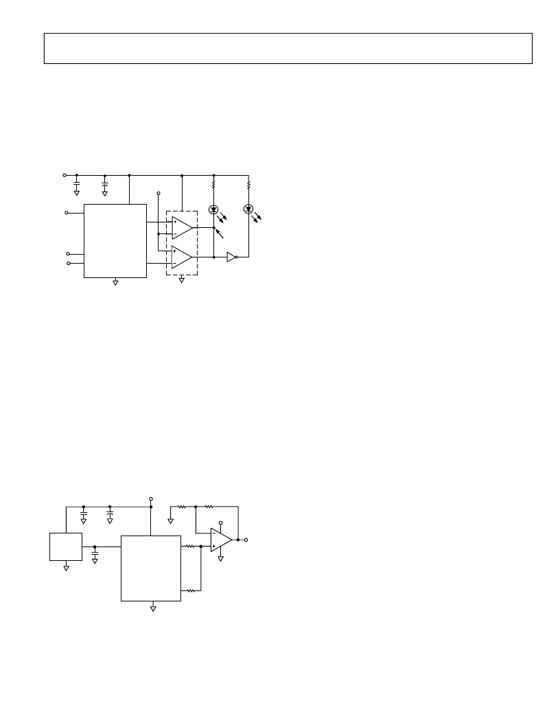
AD5337/AD5338/AD5339
PRODUCT AS A DIGITALLY PROGRAMMABLE
WINDOW DETECTOR
Figure 39 shows a digitally programmable upper/lower limit
detector using the two DACs in the AD5337/AD5338/AD5339.
The upper and lower limits for the test are loaded into DAC A
and DAC B, which, in turn, set the limits on the CMP04. If the
signal at the V
IN
input is not within the programmed window,
an LED indicates the fail condition.
Rev. A | Page 21 of 24
0
AD5337/
AD5338/
AD5339*
V
DD
5V
V
OUT
A
GND
REFIN
V
IN
PASS/FAIL
1/2
CMP04
1/6 74HC05
FAIL
PASS
1k
0.1
μ
F
SCL
SDA
SCL
DIN
1k
V
OUT
B
V
REF
*ADDITIONAL PINS OMITTED FOR CLARITY
10
μ
F
Figure 39. Window Detection
COARSE AND FINE ADJUSTMENT CAPABILITIES
The two DACs in the AD5337/AD5338/AD5339 can be paired
together to form a coarse and fine adjustment function, as
shown in Figure 40. DAC A is used to provide the coarse
adjustment while DAC B provides the fine adjustment. Varying
the ratio of R1 and R2 changes the relative effect of the coarse
and fine adjustments. With the resistor values and external
reference shown, the output amplifier has unity gain for the
DAC A output, thus the output range is 0 V to 2.5 V 1 LSB.
For DAC B the amplifier has a gain of 7.6 × 10
–3
, giving DAC B
a range equal to 19 mV.
The circuit is shown with a 2.5 V reference, but reference
voltages up to V
DD
may be used. The op amps indicated will
allow a rail-to-rail output swing.
0
1
μ
F
REFIN
V
DD
GND
V
OUT
B
0.1
μ
F
10
μ
F
V
DD
= 5V
VOUT
V
IN
GND
EXT
REF
AD820/
OP295
5V
R3
51.2k
R4
390
AD780/REF192/ADR391
WITH V
DD
= 5V
V
OUT
A
R1
390
R2
51.2k
V
OUT
AD5337/
AD5338/
AD5339*
*ADDITIONAL PINS OMITTED FOR CLARITY
Figure 40. Coarse/Fine Adjustment
POWER SUPPLY DECOUPLING
In any circuit where accuracy is important, careful consideration
of the power supply and ground return layout helps to ensure
the rated performance. The printed circuit board on which the
AD5337/AD5338/AD5339 is mounted should be designed so
that the analog and digital sections are separated and confined
to certain areas of the board. If the AD5337/AD5338/AD5339
is in a system where multiple devices require an AGND-to-
DGND connection, the connection should be made at one
point only. The star ground point should be established as close
as possible to the device. The AD5337/AD5338/AD5339 should
have ample supply bypassing of 10 μF in parallel with 0.1 μF on
the supply located as close to the package as possible, ideally
right up against the device. The 10 μF capacitors are the tantalum
bead type. The 0.1 μF capacitor should have low effective series
resistance (ESR) and low effective series inductance (ESI) to
provide a low impedance path to ground at high frequencies to
handle transient currents due to internal logic switching. The
power supply lines of the AD5337/AD5338/ AD5339 should use
as large a trace as possible to provide low impedance paths and
reduce the effects of glitches on the power supply line. Fast
switching signals such as clocks should be shielded with digital
ground to avoid radiating noise to other parts of the board, and
they should never be run near the reference inputs. A ground
line routed between the SDA and SCL lines helps to reduce
crosstalk between them. This is not required on a multilayer
board because there is a separate ground plane, but separating
the lines does help.
Avoid crossover of digital and analog signals. Traces on opposite
sides of the board should run at right angles to each other. This
reduces the effects of feedthrough through the board. Using a
microstrip technique is the best solution, but its use is not
always possible with a double-sided board. In this technique,
the component side of the board is dedicated to ground plane,
while signal traces are placed on the solder side.
相关PDF资料 |
PDF描述 |
|---|---|
| AD5339BRM-REEL | 2.5 V to 5.5 V, 250 UA, 2-Wire Interface Dual-Voltage Output, 8-/10-/12-Bit DACs |
| AD5339BRM-REEL7 | 2.5 V to 5.5 V, 250 UA, 2-Wire Interface Dual-Voltage Output, 8-/10-/12-Bit DACs |
| AD534K | Dual 14-bit 105MSPS ADC with serialized LVDS output 48-VQFN -40 to 85 |
| AD534KD | Dual 14-bit 125MSPS ADC with serialized LVDS output 48-VQFN -40 to 85 |
| AD534KH | Dual 14-bit 125MSPS ADC with serialized LVDS output 48-VQFN -40 to 85 |
相关代理商/技术参数 |
参数描述 |
|---|---|
| AD5338BRMZRMZ | 制造商:Analog Devices 功能描述:DAC,AD5338B 10bit 7us dual I2C MSOP |
| AD5338R | 制造商:AD 制造商全称:Analog Devices 功能描述:Dual, 10-Bit nanoDAC with 2 ppm/C Reference, I2C Interface |
| AD5338RBCPZ-RL7 | 功能描述:数模转换器- DAC 10-Bit 2-CH I2C w/ on-chip ref RoHS:否 制造商:Analog Devices 转换器数量:4 DAC 输出端数量:4 转换速率: 分辨率:12 bit 接口类型:Serial (I2C) 稳定时间: 最大工作温度:+ 105 C 安装风格: 封装 / 箱体:TSSOP 封装:Reel |
| AD5338RBRUZ | 功能描述:数模转换器- DAC 10-Bit 2-ch 12c nanoDAC+with on-chip ref RoHS:否 制造商:Texas Instruments 转换器数量:1 DAC 输出端数量:1 转换速率:2 MSPs 分辨率:16 bit 接口类型:QSPI, SPI, Serial (3-Wire, Microwire) 稳定时间:1 us 最大工作温度:+ 85 C 安装风格:SMD/SMT 封装 / 箱体:SOIC-14 封装:Tube |
| AD5338RBRUZ-RL7 | 功能描述:数模转换器- DAC 10-Bit 2-CH I2C w/ on-chip ref RoHS:否 制造商:Analog Devices 转换器数量: DAC 输出端数量: 转换速率: 分辨率: 接口类型: 稳定时间: 最大工作温度: 安装风格: 封装 / 箱体: 封装:Reel |
发布紧急采购,3分钟左右您将得到回复。