- 您现在的位置:买卖IC网 > PDF目录8557 > AD5381BSTZ-5-REEL (Analog Devices Inc)IC DAC 12BIT 40CH 5V 100-LQFP PDF资料下载
参数资料
| 型号: | AD5381BSTZ-5-REEL |
| 厂商: | Analog Devices Inc |
| 文件页数: | 24/40页 |
| 文件大小: | 0K |
| 描述: | IC DAC 12BIT 40CH 5V 100-LQFP |
| 产品培训模块: | Data Converter Fundamentals DAC Architectures |
| 产品变化通告: | AD5381,3 Redesign Change 24/Oct/2011 |
| 设计资源: | 40 Channels of Programmable Voltage with Excellent Temperature Drift Performance Using AD5381 (CN0010) AD5381 Channel Monitor Function (CN0013) |
| 标准包装: | 1 |
| 设置时间: | 6µs |
| 位数: | 12 |
| 数据接口: | 串行,并联 |
| 转换器数目: | 40 |
| 电压电源: | 单电源 |
| 功率耗散(最大): | 80mW |
| 工作温度: | -40°C ~ 85°C |
| 安装类型: | 表面贴装 |
| 封装/外壳: | 100-LQFP |
| 供应商设备封装: | 100-LQFP(14x14) |
| 包装: | 标准包装 |
| 输出数目和类型: | 40 电压,单极 |
| 采样率(每秒): | 167k |
| 其它名称: | AD5381BSTZ-5-REELDKR |
第1页第2页第3页第4页第5页第6页第7页第8页第9页第10页第11页第12页第13页第14页第15页第16页第17页第18页第19页第20页第21页第22页第23页当前第24页第25页第26页第27页第28页第29页第30页第31页第32页第33页第34页第35页第36页第37页第38页第39页第40页
AD5381
Data Sheet
Rev. D | Page 30 of 40
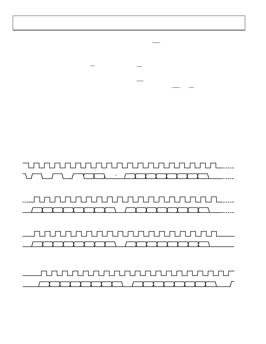
2-Byte Mode
Following initialization of 2-byte mode, the usercan update
channels sequentially. The device address byte is only required
once and the pointer address pointeris configured for auto-
increment or burst mode.
The user must begin with an addressbyte(R/W = 0), after
which the DAC acknowledges that it is preparedto receive
data by pulling SDA low. The addressbyteis followed by a
specific pointer byte (0xFF)that initiates the burst mode of
operation. The address pointer initializes to Channel 0, the data
following the pointer is loaded to Channel 0, and the address
pointer automatically incrementsto the next address.
The REG0 and REG1 bits in the data byte determinewhich
register will be updated. In this mode, following the initializa-
tion, only the two data bytes are required to updatea channel.
The channel addressautomatically increments fromAddress 0
to Channel 39 and then returns to the normal 3-bytemodeof
operation. This modeallows transmission of datato all
channels in one block and reduces the software overhead in
configuring all channels. A STOP condition at any time exits
this mode. Toggle mode is not supported in 2-byte mode.
Figure 33 shows a typical configuration.
PARALLEL INTERFACE
The SER/PAR pin must be tied low to enable the parallel
interface and disable the serial interfaces.Figure 7 shows the
timing diagram for a parallel write. The parallel interface is
controlled by the following pins.
CS Pin
Active low device select pin.
WR Pin
On the rising edge of WR, with CSlow, the addresseson Pin A5
to Pin A0 are latched; data present on the data bus is loaded into
the selected input registers.
REG0, REG1 Pins
The REG0 and REG1 pins determine the destination registerof
the data being written to the AD5381. See Table 10.
Pin A5 to Pin A0
Each of the 40 DAC channels can be individually addressed.
Pin DB11 to Pin DB0
The AD5381 accepts a straight 12-bit parallel word on DB11 to
DB0, where DB11 is the MSB and DB0 is the LSB.
1
0
1
0
1
AD1
AD0
R/W
A7 = 1
A6 = 1
A5 = 1
A4 = 1
A3 = 1
A2 = 1
A1 = 1
A0 = 1
START COND
BY MASTER
ADDRESS BYTE
POINTER BYTE
MOST SIGNIFICANT DATA BYTE
CHANNEL 0 DATA
LEAST SIGNIFICANT DATA BYTE
ACK BY
CONVERTER
MSB
ACK BY
CONVERTER
ACK BY
AD538x
ACK BY
AD538x
MOST SIGNIFICANT DATA BYTE
CHANNEL 1 DATA
LEAST SIGNIFICANT DATA BYTE
ACK BY
CONVERTER
ACK BY
CONVERTER
MOST SIGNIFICANT DATA BYTE
CHANNEL N DATA FOLLOWED BY STOP
LEAST SIGNIFICANT DATA BYTE
ACK BY
CONVERTER
ACK BY
CONVERTER
STOP
COND
BY
MASTER
REG1
REG0
MSB
LSB
MSB
LSB
REG1
REG0
MSB
LSB
MSB
LSB
REG1
REG0
MSB
LSB
MSB
LSB
SCL
SDA
SCL
SDA
SCL
SDA
SCL
SDA
03732-
033
Figure 33. 2-Byte, 12C Write Operation
相关PDF资料 |
PDF描述 |
|---|---|
| DAC8412FPC | IC DAC 12BIT QUAD READBK 28-PLCC |
| VI-JWP-MZ-B1 | CONVERTER MOD DC/DC 13.8V 25W |
| VE-B1V-MU-S | CONVERTER MOD DC/DC 5.8V 200W |
| VI-JWM-MZ-B1 | CONVERTER MOD DC/DC 10V 25W |
| VE-B1N-MU-S | CONVERTER MOD DC/DC 18.5V 200W |
相关代理商/技术参数 |
参数描述 |
|---|---|
| AD5382BST-3 | 制造商:Analog Devices 功能描述:DAC 32-CH Resistor-String 14-bit 100-Pin LQFP 制造商:Rochester Electronics LLC 功能描述:32/40-CHANNEL 3V/5V SINGLE SUPPLY 12/14-BIT VOUT DAC - Bulk |
| AD5382BST-3-REEL | 制造商:Analog Devices 功能描述:DAC 32-CH Resistor-String 14-bit 100-Pin LQFP T/R |
| AD5382BST-5 | 制造商:Analog Devices 功能描述:DAC 32-CH Resistor-String 14-bit 100-Pin LQFP 制造商:Rochester Electronics LLC 功能描述:32-CHN 5V SINGLE SUPPLY 14-BIT VOUT I.C. - Bulk |
| AD5382BST-5-REEL | 制造商:Analog Devices 功能描述:DAC 32-CH Resistor-String 14-bit 100-Pin LQFP T/R |
| AD5382BSTZ-3 | 功能描述:IC DAC 14BIT 32CHAN 3V 100LQFP RoHS:是 类别:集成电路 (IC) >> 数据采集 - 数模转换器 系列:- 产品培训模块:Lead (SnPb) Finish for COTS Obsolescence Mitigation Program 标准包装:1,000 系列:- 设置时间:1µs 位数:8 数据接口:串行 转换器数目:8 电压电源:双 ± 功率耗散(最大):941mW 工作温度:0°C ~ 70°C 安装类型:表面贴装 封装/外壳:24-SOIC(0.295",7.50mm 宽) 供应商设备封装:24-SOIC W 包装:带卷 (TR) 输出数目和类型:8 电压,单极 采样率(每秒):* |
发布紧急采购,3分钟左右您将得到回复。