- 您现在的位置:买卖IC网 > PDF目录8557 > AD5381BSTZ-5-REEL (Analog Devices Inc)IC DAC 12BIT 40CH 5V 100-LQFP PDF资料下载
参数资料
| 型号: | AD5381BSTZ-5-REEL |
| 厂商: | Analog Devices Inc |
| 文件页数: | 28/40页 |
| 文件大小: | 0K |
| 描述: | IC DAC 12BIT 40CH 5V 100-LQFP |
| 产品培训模块: | Data Converter Fundamentals DAC Architectures |
| 产品变化通告: | AD5381,3 Redesign Change 24/Oct/2011 |
| 设计资源: | 40 Channels of Programmable Voltage with Excellent Temperature Drift Performance Using AD5381 (CN0010) AD5381 Channel Monitor Function (CN0013) |
| 标准包装: | 1 |
| 设置时间: | 6µs |
| 位数: | 12 |
| 数据接口: | 串行,并联 |
| 转换器数目: | 40 |
| 电压电源: | 单电源 |
| 功率耗散(最大): | 80mW |
| 工作温度: | -40°C ~ 85°C |
| 安装类型: | 表面贴装 |
| 封装/外壳: | 100-LQFP |
| 供应商设备封装: | 100-LQFP(14x14) |
| 包装: | 标准包装 |
| 输出数目和类型: | 40 电压,单极 |
| 采样率(每秒): | 167k |
| 其它名称: | AD5381BSTZ-5-REELDKR |
第1页第2页第3页第4页第5页第6页第7页第8页第9页第10页第11页第12页第13页第14页第15页第16页第17页第18页第19页第20页第21页第22页第23页第24页第25页第26页第27页当前第28页第29页第30页第31页第32页第33页第34页第35页第36页第37页第38页第39页第40页
AD5381
Data Sheet
Rev. D | Page 34 of 40
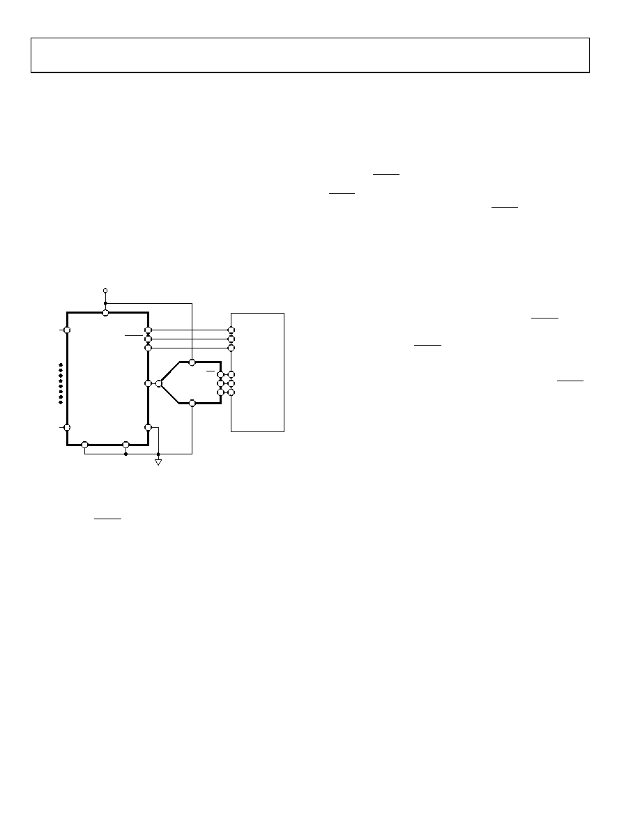
MONITOR FUNCTION
The AD5381 channel monitor function consists of a multiplexer
addressedvia the interface, allowing any channel output to be
routed to this pin for monitoring using an external ADC. In
channel monitor mode, VOUT39 becomes the MON_OUTpin,
to which all monitoredsignals are routed. The channel monitor
function must be enabled in the control register beforeany
channels are routed to MON_OUT. Table17 contains the
decoding information required to route anychannel to
MON_OUT.Selecting Channel Address 63 three-states
MON_OUT.Figure 41 shows a typical monitoring circuit
implemented using a 12-bit SAR ADC in a 6-lead SOT-23
package. The controller output port selects the channel to be
monitored, and the input port readsthe converteddata from
the ADC.
AD7476
GND
SDATA
CS
SCLK
VDD
VIN
VOUT39/MON_OUT
AGND
DIN
SYNC
SCLK
DAC_GND SIGNAL_GND
VOUT0
VOUT38
AVDD
AD5381
OUTPUT PORT
INPUT PORT
CONTROLLER
03732-041
Figure 41. Typical Channel Monitoring Circuit
TOGGLE MODE FUNCTION
The toggle mode function allows an output signal to be gener-
ated using the LDACcontrolsignalthat switches between two
DAC data registers. This function is configured using the SFR
control register as follows. A write with REG1 = REG0 = 0 and
A5 to A0 = 001100 specifies a control register write. The toggle
mode function is enabled in groups of eight channels using Bit
CR4 to Bit CR0 in the control register. See the AD5381 control
register description. Figure42 shows a blockdiagram of toggle
mode implementation. Each of the 40 DAC channels on the
AD5381 contain an A and B data register.
Note that B registers can only be loadedwhen toggle mode is
enabled. The sequence of events whenconfiguring the AD5381
for toggle mode is
1. Enable toggle mode for the required channels via the
control register.
2. Load data to the A registers.
3. Load data to the B registers.
4. Apply LDAC.
LDACis used to switch between the A and B registers in
determining the analog output. Thefirst LDACconfiguresthe
output to reflect data in the A registers. This modeofferssignif-
icant advantages if the user wants to generatea square waveat
the output of all 40 channels, as might be required to drivea
liquid crystal-based variableoptical attenuator.
In this case, the user writes to the control register and enables
the toggle function by setting CR4 to CR2 = 0, thus enabling the
five groups of eight for toggle modeoperation. The user must
then load data to all 40 A and B registers. Toggling LDACsets
the output values to reflect the data in the A and B registers.
The frequency of the LDACdetermines the frequency of the
square waveoutput.
Toggle mode is disabled via the control register. The first LDAC
following the disabling of the toggle mode will update the out-
puts with the data contained in the A registers.
THERMAL MONITOR FUNCTION
The AD5381 contains a temperature shutdown function to
protect the chip if multiple outputs areshorted. The short-
circuit current of each output amplifier is typically 40 mA.
Operating the AD5381 at 5 V leads to a power dissipation of
200 mW per shorted amplifier. Withfive channels shorted, this
leads to an extra watt of powerdissipation. Forthe 100-lead
LQFP, the θ
JA is typically 44°C/W.
The thermal monitoris enabledby the user via CR6 in the
control register. The outputamplifiers on the AD5381 are
automatically powered down if the die temperatureexceeds
approximately 130°C. After a thermal shutdown hasoccurred,
the user can re-enable the part by executing a soft power-upif
the temperature has droppedbelow130°C or by turning off the
thermal monitorfunction via the control register.
相关PDF资料 |
PDF描述 |
|---|---|
| DAC8412FPC | IC DAC 12BIT QUAD READBK 28-PLCC |
| VI-JWP-MZ-B1 | CONVERTER MOD DC/DC 13.8V 25W |
| VE-B1V-MU-S | CONVERTER MOD DC/DC 5.8V 200W |
| VI-JWM-MZ-B1 | CONVERTER MOD DC/DC 10V 25W |
| VE-B1N-MU-S | CONVERTER MOD DC/DC 18.5V 200W |
相关代理商/技术参数 |
参数描述 |
|---|---|
| AD5382BST-3 | 制造商:Analog Devices 功能描述:DAC 32-CH Resistor-String 14-bit 100-Pin LQFP 制造商:Rochester Electronics LLC 功能描述:32/40-CHANNEL 3V/5V SINGLE SUPPLY 12/14-BIT VOUT DAC - Bulk |
| AD5382BST-3-REEL | 制造商:Analog Devices 功能描述:DAC 32-CH Resistor-String 14-bit 100-Pin LQFP T/R |
| AD5382BST-5 | 制造商:Analog Devices 功能描述:DAC 32-CH Resistor-String 14-bit 100-Pin LQFP 制造商:Rochester Electronics LLC 功能描述:32-CHN 5V SINGLE SUPPLY 14-BIT VOUT I.C. - Bulk |
| AD5382BST-5-REEL | 制造商:Analog Devices 功能描述:DAC 32-CH Resistor-String 14-bit 100-Pin LQFP T/R |
| AD5382BSTZ-3 | 功能描述:IC DAC 14BIT 32CHAN 3V 100LQFP RoHS:是 类别:集成电路 (IC) >> 数据采集 - 数模转换器 系列:- 产品培训模块:Lead (SnPb) Finish for COTS Obsolescence Mitigation Program 标准包装:1,000 系列:- 设置时间:1µs 位数:8 数据接口:串行 转换器数目:8 电压电源:双 ± 功率耗散(最大):941mW 工作温度:0°C ~ 70°C 安装类型:表面贴装 封装/外壳:24-SOIC(0.295",7.50mm 宽) 供应商设备封装:24-SOIC W 包装:带卷 (TR) 输出数目和类型:8 电压,单极 采样率(每秒):* |
发布紧急采购,3分钟左右您将得到回复。