参数资料
| 型号: | AD5382BSTZ-3 |
| 厂商: | Analog Devices Inc |
| 文件页数: | 26/40页 |
| 文件大小: | 0K |
| 描述: | IC DAC 14BIT 32CHAN 3V 100LQFP |
| 产品培训模块: | Data Converter Fundamentals DAC Architectures |
| 产品变化通告: | Redesign Change 28/Oct/2011 |
| 设计资源: | 32 Channels of Programmable Voltage with Excellent Temperature Drift Performance Using AD5382 (CN0011) AD5382 Channel Monitor Function (CN0012) |
| 标准包装: | 1 |
| 设置时间: | 8µs |
| 位数: | 14 |
| 数据接口: | 串行,并联 |
| 转换器数目: | 32 |
| 电压电源: | 单电源 |
| 功率耗散(最大): | 65mW |
| 工作温度: | -40°C ~ 85°C |
| 安装类型: | 表面贴装 |
| 封装/外壳: | 100-LQFP |
| 供应商设备封装: | 100-LQFP(14x14) |
| 包装: | 托盘 |
| 输出数目和类型: | 32 电压,单极 |
| 采样率(每秒): | 125k |
第1页第2页第3页第4页第5页第6页第7页第8页第9页第10页第11页第12页第13页第14页第15页第16页第17页第18页第19页第20页第21页第22页第23页第24页第25页当前第26页第27页第28页第29页第30页第31页第32页第33页第34页第35页第36页第37页第38页第39页第40页
AD5382
Data Sheet
Rev. C | Page 32 of 40
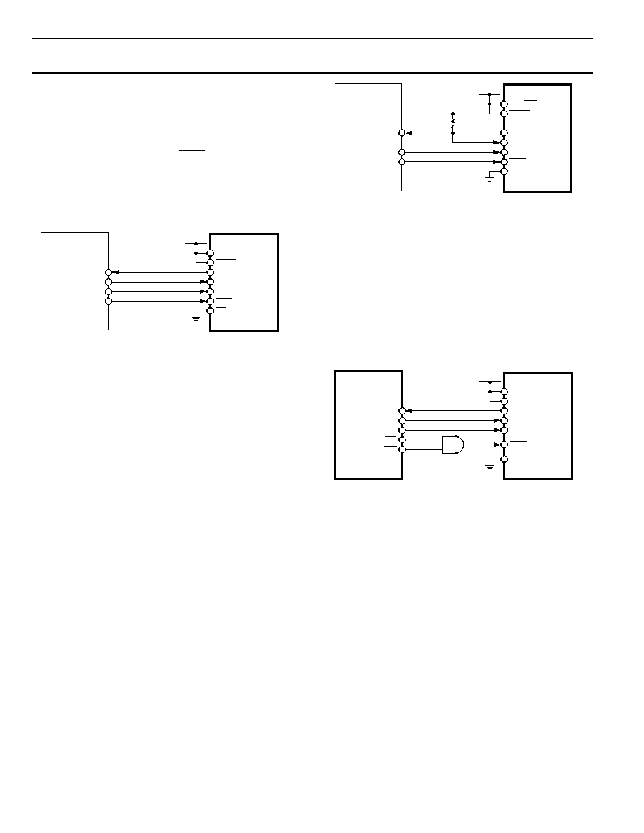
AD5382 to PIC16C6x/7x
The PIC16C6x/7x synchronous serial port (SSP) is configured as
an SPI master with the Clock Polarity bit = 0. This is done by
writing to the synchronous serial port control register (SSPCON).
See the PIC16/17 Microcontroller User Manual. In this example
I/O, Port RA1 is being used to pulse SYNC and enable the serial
port of the AD5382. This microcontroller transfers only eight
bits of data during each serial transfer operation; therefore, three
consecutive read/write operations may be needed depending on
the mode. Figure 35 shows the connection diagram.
03733-036
PIC16C6X/7X1
AD53821
SDI/RC4
SDO/RC5
SCK/RC3
RA1
SDO
RESET
SER/PAR
DIN
SCLK
SYNC
SPI/I2C
DVDD
1ADDITIONAL PINS OMITTED FOR CLARITY.
Figure 35. AD5382-to-PIC16C6x/7x Interface
AD5382 to 8051
The AD5382 requires a clock synchronized to the serial data.
The 8051 serial interface must therefore be operated in Mode 0.
In this mode, serial data enters and exits through RxD, and a
shift clock is output on TxD. Figure 36 shows how the 8051 is
connected to the AD5382. Because the AD5382 shifts data out
on the rising edge of the shift clock and latches data in on the
falling edge, the shift clock must be inverted. The AD5382
requires its data to be MSB first. Since the 8051 outputs the
LSB first, the transmit routine must take this into account.
03733-037
8XC511
AD53821
RxD
TxD
P1.1
SDO
RESET
SER/PAR
DIN
SCLK
SYNC
SPI/I2C
DVDD
1ADDITIONAL PINS OMITTED FOR CLARITY.
Figure 36. AD5382-to-8051 Interface
AD5382 to ADSP-2101/ADSP-2103
Figure 37 shows a serial interface between the AD5382 and the
ADSP-2101/ADSP-2103. The ADSP-2101/ADSP-2103 should
be set up to operate in SPORT transmit alternate framing mode.
The ADSP-2101/ADSP-2103 SPORT is programmed through
the SPORT control register and should be configured as follows:
internal clock operation, active low framing, and 16-bit word
length. Transmission is initiated by writing a word to the
Tx register after the SPORT has been enabled.
03733-038
ADSP-2101/
ADSP-21031
AD53821
DR
DT
SCK
TFS
RFS
SDO
RESET
SER/PAR
DIN
SCLK
DVDD
SPI/I2C
SYNC
1ADDITIONAL PINS OMITTED FOR CLARITY.
Figure 37. AD5382-to-ADSP-2101/ADSP-2103 Interface
相关PDF资料 |
PDF描述 |
|---|---|
| AD5390BCPZ-5 | IC DAC 14BIT 16CHAN 5V 64LFCSP |
| AD5398ABCBZ-REEL | IC DAC 10BIT CURRENT-SINK 9WLCSP |
| AD5405YCPZ-REEL7 | IC DAC DUAL 12BIT MULT 40LFCSP |
| AD5415YRU | IC DAC DUAL 12BIT MULT 24-TSSOP |
| AD5421CREZ | IC DAC 16BIT SPI/SRL 28TSSOP |
相关代理商/技术参数 |
参数描述 |
|---|---|
| AD5382BSTZ-5 | 功能描述:IC DAC 14BIT 32CH 5V 100-LQFP RoHS:是 类别:集成电路 (IC) >> 数据采集 - 数模转换器 系列:- 产品培训模块:Lead (SnPb) Finish for COTS Obsolescence Mitigation Program 标准包装:1,000 系列:- 设置时间:1µs 位数:8 数据接口:串行 转换器数目:8 电压电源:双 ± 功率耗散(最大):941mW 工作温度:0°C ~ 70°C 安装类型:表面贴装 封装/外壳:24-SOIC(0.295",7.50mm 宽) 供应商设备封装:24-SOIC W 包装:带卷 (TR) 输出数目和类型:8 电压,单极 采样率(每秒):* |
| AD5383BST | 制造商:Analog Devices 功能描述:- Bulk |
| AD5383BST-3 | 制造商:Rochester Electronics LLC 功能描述:32/40-CHANNEL 3V/5V SINGLE SUPPLY 12/14-BIT VOUT DAC - Bulk 制造商:Analog Devices 功能描述: |
| AD5383BST-5 | 制造商:Analog Devices 功能描述:DAC 32-CH Resistor-String 12-bit 100-Pin LQFP 制造商:Rochester Electronics LLC 功能描述:32-CHN 5V SINGLE SUPPLY 12-BIT VOUT I.C. - Bulk |
| AD5383BST-5-REEL | 制造商:Analog Devices 功能描述:DAC 32-CH Resistor-String 12-bit 100-Pin LQFP T/R |
发布紧急采购,3分钟左右您将得到回复。