参数资料
| 型号: | AD5383BSTZ-5 |
| 厂商: | Analog Devices Inc |
| 文件页数: | 25/40页 |
| 文件大小: | 0K |
| 描述: | IC DAC 12BIT 32CH 5V 100-LQFP |
| 产品培训模块: | Data Converter Fundamentals DAC Architectures |
| 产品变化通告: | AD5381,3 Redesign Change 24/Oct/2011 |
| 设计资源: | 32 Channels of Programmable Voltage with Excellent Temperature Drift Performance Using AD5383 (CN0014) AD5383 Channel Monitor Function (CN0015) |
| 标准包装: | 1 |
| 设置时间: | 6µs |
| 位数: | 12 |
| 数据接口: | 串行,并联 |
| 转换器数目: | 32 |
| 电压电源: | 单电源 |
| 功率耗散(最大): | 65mW |
| 工作温度: | -40°C ~ 85°C |
| 安装类型: | 表面贴装 |
| 封装/外壳: | 100-LQFP |
| 供应商设备封装: | 100-LQFP(14x14) |
| 包装: | 托盘 |
| 输出数目和类型: | 32 电压,单极;32 电压,双极 |
| 采样率(每秒): | 167k |
第1页第2页第3页第4页第5页第6页第7页第8页第9页第10页第11页第12页第13页第14页第15页第16页第17页第18页第19页第20页第21页第22页第23页第24页当前第25页第26页第27页第28页第29页第30页第31页第32页第33页第34页第35页第36页第37页第38页第39页第40页
Data Sheet
AD5383
Rev. C | Page 31 of 40
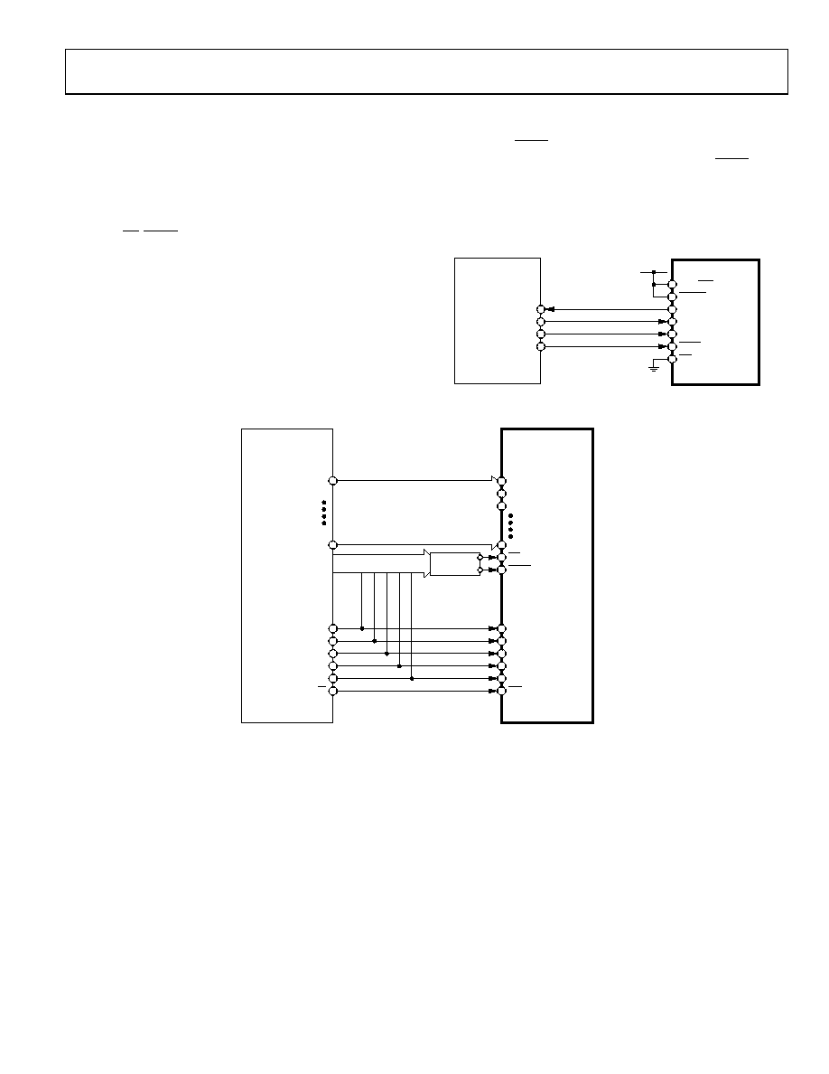
MICROPROCESSOR INTERFACING
Parallel Interface
The AD5383 can be interfaced to a variety of 16-bit microcon-
trollers or DSP processors. Figure 35 shows the AD5383 family
interfaced to a generic 16-bit microcontroller/DSP processor. The
lower address lines from the processor are connected to A0 to
A4 on the AD5383. The upper address lines are decoded to
provide a CS, LDAC signal for the AD5383. The fast interface
timing of the AD5383 allows direct interface to a wide variety of
microcontrollers and DSPs, as shown in Figure 35.
AD5383 to MC68HC11
The serial peripheral interface (SPI) on the MC68HC11 is
configured for master mode (MSTR = 1), the clock polarity bit
(CPOL) = 0, and the clock phase bit (CPHA) = 1. The SPI is
configured by writing to the SPI control register (SPCR)—see
the 68HC11 User Manual. SCK of the 68HC11 drives the SCLK
of the AD5383, the MOSI output drives the serial data line
(DIN) of the AD5383, and the MISO input is driven from
DOUT. The SYNC signal is derived from a port line (PC7).
When data is being transmitted to the AD5383, the SYNC line
is taken low (PC7). Data appearing on the MOSI output is valid
on the falling edge of SCK. Serial data from the 68HC11 is
transmitted in 8-bit bytes with only eight falling clock edges
occurring in the transmit cycle.
03734-034
MC68HC11
AD5383
MISO
MOSI
SCK
PC7
SDO
RESET
SER/PAR
DIN
SCLK
SYNC
SPI/I2C
DVDD
Figure 34. AD5383-to-MC68HC11 Interface
03734-035
CONTROLLER/
DSP PROCESSOR*
AD5383
ADDRESS
DECODE
UPPER BITS OF
ADDRESS BUS
DATA
BUS
D15
D0
A4
A3
A2
A1
A0
R/W
A4
A3
A2
A1
A0
WR
REG1
REG0
D11
D0
CS
LDAC
*ADDITIONAL PINS OMITTED FOR CLARITY
Figure 35. AD5383-to-Parallel Interface
相关PDF资料 |
PDF描述 |
|---|---|
| AD5384BBCZ-5 | IC DAC 14BIT 40CH 5V 100-CSPBGA |
| AD5398BCPZ-REEL | IC DAC 10BIT CURRENT-SINK 8LFCSP |
| AD5420AREZ-REEL7 | IC DAC 16BIT 1CH SER 24TSSOP |
| AD5425YRM | IC DAC MULTIPLYING 8BIT 10-MSOP |
| AD5443YRM | IC DAC 12BIT SERIAL IOUT 10-MSOP |
相关代理商/技术参数 |
参数描述 |
|---|---|
| AD5384BBC-3 | 功能描述:IC DAC 14BIT 40CH 3V 100-CSPBGA RoHS:否 类别:集成电路 (IC) >> 数据采集 - 数模转换器 系列:- 标准包装:2,400 系列:- 设置时间:- 位数:18 数据接口:串行 转换器数目:3 电压电源:模拟和数字 功率耗散(最大):- 工作温度:-40°C ~ 85°C 安装类型:表面贴装 封装/外壳:36-TFBGA 供应商设备封装:36-TFBGA 包装:带卷 (TR) 输出数目和类型:* 采样率(每秒):* |
| AD5384BBC-3REEL7 | 功能描述:IC DAC 14BIT 40CH 3V 100-CSPBGA RoHS:否 类别:集成电路 (IC) >> 数据采集 - 数模转换器 系列:- 标准包装:2,400 系列:- 设置时间:- 位数:18 数据接口:串行 转换器数目:3 电压电源:模拟和数字 功率耗散(最大):- 工作温度:-40°C ~ 85°C 安装类型:表面贴装 封装/外壳:36-TFBGA 供应商设备封装:36-TFBGA 包装:带卷 (TR) 输出数目和类型:* 采样率(每秒):* |
| AD5384BBC-5 | 功能描述:IC DAC 14BIT 40CH 5V 100-CSPBGA RoHS:否 类别:集成电路 (IC) >> 数据采集 - 数模转换器 系列:- 标准包装:2,400 系列:- 设置时间:- 位数:18 数据接口:串行 转换器数目:3 电压电源:模拟和数字 功率耗散(最大):- 工作温度:-40°C ~ 85°C 安装类型:表面贴装 封装/外壳:36-TFBGA 供应商设备封装:36-TFBGA 包装:带卷 (TR) 输出数目和类型:* 采样率(每秒):* |
| AD5384BBC-5REEL7 | 功能描述:IC DAC 14BIT 40CH 5V 100-CSPBGA RoHS:否 类别:集成电路 (IC) >> 数据采集 - 数模转换器 系列:- 标准包装:2,400 系列:- 设置时间:- 位数:18 数据接口:串行 转换器数目:3 电压电源:模拟和数字 功率耗散(最大):- 工作温度:-40°C ~ 85°C 安装类型:表面贴装 封装/外壳:36-TFBGA 供应商设备封装:36-TFBGA 包装:带卷 (TR) 输出数目和类型:* 采样率(每秒):* |
| AD5384BBCZ-3 | 功能描述:IC DAC 14BIT 40CH 5V 100-CSPBGA RoHS:是 类别:集成电路 (IC) >> 数据采集 - 数模转换器 系列:- 标准包装:2,400 系列:- 设置时间:- 位数:18 数据接口:串行 转换器数目:3 电压电源:模拟和数字 功率耗散(最大):- 工作温度:-40°C ~ 85°C 安装类型:表面贴装 封装/外壳:36-TFBGA 供应商设备封装:36-TFBGA 包装:带卷 (TR) 输出数目和类型:* 采样率(每秒):* |
发布紧急采购,3分钟左右您将得到回复。