- 您现在的位置:买卖IC网 > PDF目录10784 > AD5384BBCZ-3 (Analog Devices Inc)IC DAC 14BIT 40CH 5V 100-CSPBGA PDF资料下载
参数资料
| 型号: | AD5384BBCZ-3 |
| 厂商: | Analog Devices Inc |
| 文件页数: | 11/32页 |
| 文件大小: | 0K |
| 描述: | IC DAC 14BIT 40CH 5V 100-CSPBGA |
| 产品培训模块: | Data Converter Fundamentals DAC Architectures |
| 产品变化通告: | AD5384 Models Discontinuation 15/May/2012 |
| 标准包装: | 1 |
| 设置时间: | 8µs |
| 位数: | 14 |
| 数据接口: | 串行 |
| 转换器数目: | 40 |
| 电压电源: | 单电源 |
| 功率耗散(最大): | 80mW |
| 工作温度: | -40°C ~ 85°C |
| 安装类型: | 表面贴装 |
| 封装/外壳: | 100-LFBGA,CSPBGA |
| 供应商设备封装: | 100-CSBGA(10x10) |
| 包装: | 托盘 |
| 输出数目和类型: | 40 电压,单极 |
| 采样率(每秒): | 125k |
第1页第2页第3页第4页第5页第6页第7页第8页第9页第10页当前第11页第12页第13页第14页第15页第16页第17页第18页第19页第20页第21页第22页第23页第24页第25页第26页第27页第28页第29页第30页第31页第32页
Data Sheet
AD5384
FUNCTIONAL DESCRIPTION
DAC ARCHITECTURE—GENERAL
The AD5384 is a complete single-supply, 40-channel, voltage
output DAC offering 14-bit resolution, available in a 100-lead
CSP_BGA package. It features two serial interfaces, SPI and
I2C. This family includes an internal 1.25 V/2.5 V, 10 ppm/°C
that drives the buffered reference inputs. Alternatively, an
external reference can drive these inputs. Reference selection is
via a bit in the control register. Internal/external reference
selection is via the CR10 bit in the control register, and the
CR12 bit in the control register selects the reference magnitude
if the internal reference is selected. All channels have an on-chip
output amplifier with rail-to-rail output capable of driving 5 k
in parallel with a 200 pF load.
The architecture of a single DAC channel consists of a 14-bit
resistor string DAC followed by an output buffer amplifier
operating at a gain of 2. This resistor string architecture
guarantees DAC monotonicity. The 14-bit binary digital code
loaded to the DAC register determines at which node on the
string the voltage is tapped off before being fed to the output
amplifier.
Each channel on these devices contains independent offset and
gain control registers allowing the user to digitally trim offset
and gain. These registers let the user calibrate out errors in the
complete signal chain, including the DAC, using the internal m
and c registers that hold the correction factors. All channels are
double buffered, allowing synchronous updating of all channels
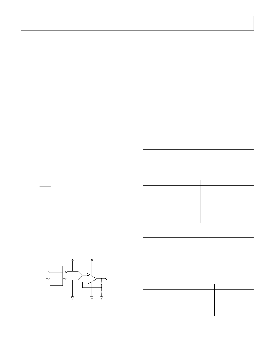
using the LDAC pin. Figure 24 shows a block diagram of a
single channel on the AD5384. The following represents the
digital input transfer function for each DAC:
x2 = [(m + 2)/ 2n× x1] + (c – 2n– 1)
where:
x2 is the data-word loaded to the resistor-string DAC.
x1 is the 14-bit data-word written to the DAC input register.
m is the gain coefficient (default is 0x3FFE on the AD5384).
The gain coefficient is written to the 13 most significant bits
(DB13 to DB1) and the LSB (DB0) is 0.
n is the DAC resolution (n = 14 for AD5384).
c is the14-bit offset coefficient (default is 0x2000).
VOUTx
R
14-BIT
DAC
m REG
c REG
×1 INPUT
REG
×2
INPUT DATA
VREF (+)
AVDDx
AGND
04652-
026
Figure 24. Single-Channel Architecture
The following represents the complete transfer function for
these devices:
VOUT = 2 × VREF × x2/2n
where:
x2 is the data-word loaded to the resistor string DAC.
VREF is the internal reference voltage or the reference voltage
externally applied to the DAC REF_OUT/REF_IN pin. For
specified performance, an external reference voltage of 2.5 V is
recommended.
DATA DECODING
The AD5384 contains a 14-bit data bus, DB13 to DB0.
Depending on the value of REG1 and REG0 outlined in Table 7,
this data is loaded into the addressed DAC input register(s),
offset (c) register(s), or gain (m) register(s). Table 8, Table 9,
and Table 10 outline the contents of the format data, offset (c),
and gain (m) registers.
Table 7. Register Selection
REG1
REG0
Register Selected
1
Input data register (×1)
1
0
Offset register (c)
0
1
Gain register (m)
0
Special function registers (SFRs)
Table 8. DAC Data Format (REG1 = 1, REG0 = 1)
DB13 to DB0
DAC Output (V)
11
1111
2 VREF × (16383/16384)
11
1111
1110
2 VREF × (16382/16384)
10
0000
0001
2 VREF × (8193/16384)
10
0000
2 VREF × (8192/16384)
01
1111
2 VREF × (8191/16384)
00
0000
0001
2 VREF × (1/16384)
00
0000
0
Table 9. Offset Data Format (REG1 = 1, REG0 = 0)
DB13 to DB0
Offset (LSB)
11
1111
+8191
11
1111
1110
+8190
10
0000
0001
+1
10
0000
0
01
1111
–1
00
0000
0001
–8191
00
0000
–8192
Table 10. Gain Data Format (REG1 = 0, REG0 = 1)
DB13 to DB0
Gain Factor
11
1111
1110
1
10
1111
1110
0.75
01
1111
1110
0.5
00
1111
1110
0.25
00
0000
0
Rev. B | Page 19 of 32
相关PDF资料 |
PDF描述 |
|---|---|
| VE-J0H-MY-S | CONVERTER MOD DC/DC 52V 50W |
| VI-B42-IV-S | CONVERTER MOD DC/DC 15V 150W |
| VI-2WW-IW-S | CONVERTER MOD DC/DC 5.5V 100W |
| VE-JTL-MY-S | CONVERTER MOD DC/DC 28V 50W |
| VE-J0F-MY-S | CONVERTER MOD DC/DC 72V 50W |
相关代理商/技术参数 |
参数描述 |
|---|---|
| AD5384BBCZ-5 | 功能描述:IC DAC 14BIT 40CH 5V 100-CSPBGA RoHS:是 类别:集成电路 (IC) >> 数据采集 - 数模转换器 系列:- 标准包装:2,400 系列:- 设置时间:- 位数:18 数据接口:串行 转换器数目:3 电压电源:模拟和数字 功率耗散(最大):- 工作温度:-40°C ~ 85°C 安装类型:表面贴装 封装/外壳:36-TFBGA 供应商设备封装:36-TFBGA 包装:带卷 (TR) 输出数目和类型:* 采样率(每秒):* |
| AD5384BBCZ-5REEL7 | 功能描述:14 Bit Digital to Analog Converter 40 100-CSBGA (10x10) 制造商:analog devices inc. 系列:denseDAC 包装:带卷(TR) 零件状态:有效 位数:14 数模转换器数:40 建立时间:8μs 输出类型:Voltage - Buffered 差分输出:无 数据接口:I2C,SPI,DSP 参考类型:外部, 内部 电压 - 电源,模拟:5V 电压 - 电源,数字:2.7 V ~ 5.5 V INL/DNL(LSB):±4(最大),-1/+2(最大) 架构:电阻串 DAC 工作温度:-40°C ~ 85°C 封装/外壳:100-LFBGA,CSPBGA 供应商器件封装:100-CSBGA(10x10) 标准包装:400 |
| AD538AD | 功能描述:IC MULT/DIV REALTIME ACU 18-CDIP RoHS:否 类别:集成电路 (IC) >> 线性 - 模拟乘法器,除法器 系列:- 标准包装:25 系列:HA 功能:模拟乘法器 位元/级数:四象限 封装/外壳:16-CDIP(0.300",7.62mm) 供应商设备封装:16-CDIP 侧面铜焊 包装:管件 |
| AD538ADZ | 功能描述:IC REALTIME ACU UNIT 18-CDIP RoHS:是 类别:集成电路 (IC) >> 线性 - 模拟乘法器,除法器 系列:- 标准包装:25 系列:HA 功能:模拟乘法器 位元/级数:四象限 封装/外壳:16-CDIP(0.300",7.62mm) 供应商设备封装:16-CDIP 侧面铜焊 包装:管件 |
| AD538BD | 功能描述:IC MULT/DIV REALTIME ACU 18-CDIP RoHS:否 类别:集成电路 (IC) >> 线性 - 模拟乘法器,除法器 系列:- 标准包装:25 系列:HA 功能:模拟乘法器 位元/级数:四象限 封装/外壳:16-CDIP(0.300",7.62mm) 供应商设备封装:16-CDIP 侧面铜焊 包装:管件 |
发布紧急采购,3分钟左右您将得到回复。