- 您现在的位置:买卖IC网 > PDF目录10784 > AD5384BBCZ-3 (Analog Devices Inc)IC DAC 14BIT 40CH 5V 100-CSPBGA PDF资料下载
参数资料
| 型号: | AD5384BBCZ-3 |
| 厂商: | Analog Devices Inc |
| 文件页数: | 19/32页 |
| 文件大小: | 0K |
| 描述: | IC DAC 14BIT 40CH 5V 100-CSPBGA |
| 产品培训模块: | Data Converter Fundamentals DAC Architectures |
| 产品变化通告: | AD5384 Models Discontinuation 15/May/2012 |
| 标准包装: | 1 |
| 设置时间: | 8µs |
| 位数: | 14 |
| 数据接口: | 串行 |
| 转换器数目: | 40 |
| 电压电源: | 单电源 |
| 功率耗散(最大): | 80mW |
| 工作温度: | -40°C ~ 85°C |
| 安装类型: | 表面贴装 |
| 封装/外壳: | 100-LFBGA,CSPBGA |
| 供应商设备封装: | 100-CSBGA(10x10) |
| 包装: | 托盘 |
| 输出数目和类型: | 40 电压,单极 |
| 采样率(每秒): | 125k |
第1页第2页第3页第4页第5页第6页第7页第8页第9页第10页第11页第12页第13页第14页第15页第16页第17页第18页当前第19页第20页第21页第22页第23页第24页第25页第26页第27页第28页第29页第30页第31页第32页
AD5384
Data Sheet
I2C SERIAL INTERFACE
of a serial data line (SDA) and a serial clock line (SCL). SDA and
SCL facilitate communication between the AD5384 and the master
at rates up to 400 kHz. Figure 6 shows the 2-wire interface timing
diagrams that incorporate three different modes of operation.
Select I2C mode by configuring the SPI/I2C pin to a Logic 0. The
device is connected to this bus as a slave device, and no clock is
generated by the AD5384. The AD5384 has a 7-bit slave address,
1010 1 (AD1)(AD0) The 5 MSBs are hard coded, and the two LSBs
are determined by the state of the AD1 and AD0 pins. The ability
to hardware-configure AD1 and AD0 allows four of these devices
to be configured on the bus.
I2C Data Transfer
During each SCL clock cycle, one data bit transfers. The data on
SDA must remain stable during the high period of the SCL clock
pulse. Changes in SDA while SCL is high are control signals that
configure start and stop conditions. When the I2C bus is not busy,
the external pull-up resistors pull both SDA and SCL high.
Start and Stop Conditions
A master device initiates communication by issuing a start
condition. A start condition is a high to low transition on SDA with
SCL high. A stop condition is a low to high transition on SDA
while SCL is high. A start condition from the master signals the
beginning of a transmission to the AD5384. The stop condition
frees the bus. If a repeated start condition (Sr) generates instead of a
stop condition, the bus remains active.
Repeated Start Conditions
A repeated start (Sr) condition can indicate a change of data
direction on the bus. Use Sr when the bus master is writing to
several I2C devices and wants to maintain control of the bus.
Acknowledge Bit (ACK)
The acknowledge bit (ACK) is the ninth bit attached to any
8-bit data-word. ACK is always generated by the receiving device.
The AD5384 devices generate an ACK when receiving an address
or data by pulling SDA low during the ninth clock period.
Monitoring ACK allows detection of unsuccessful data transfers.
An unsuccessful data transfer occurs if a receiving device is busy or
if a system fault occurs. In the event of an unsuccessful data
transfer, the bus master reattempts communication.
Slave Addresses
A bus master initiates communication with a slave device by
issuing a start condition, followed by the 7-bit slave address.
When idle, the AD5384 waits for a start condition followed by its
slave address. The LSB of the address word is the read/write (R/W)
bit. The AD5384 devices are receive-only devices; when
communicating with these, R/W = 0. After receiving the proper
address 1010 1(AD1)(AD0), the AD5384 issues an ACK by pulling
SDA low for one clock cycle.
The AD5384 has four different user programmable addresses
determined by the AD1 and AD0 bits.
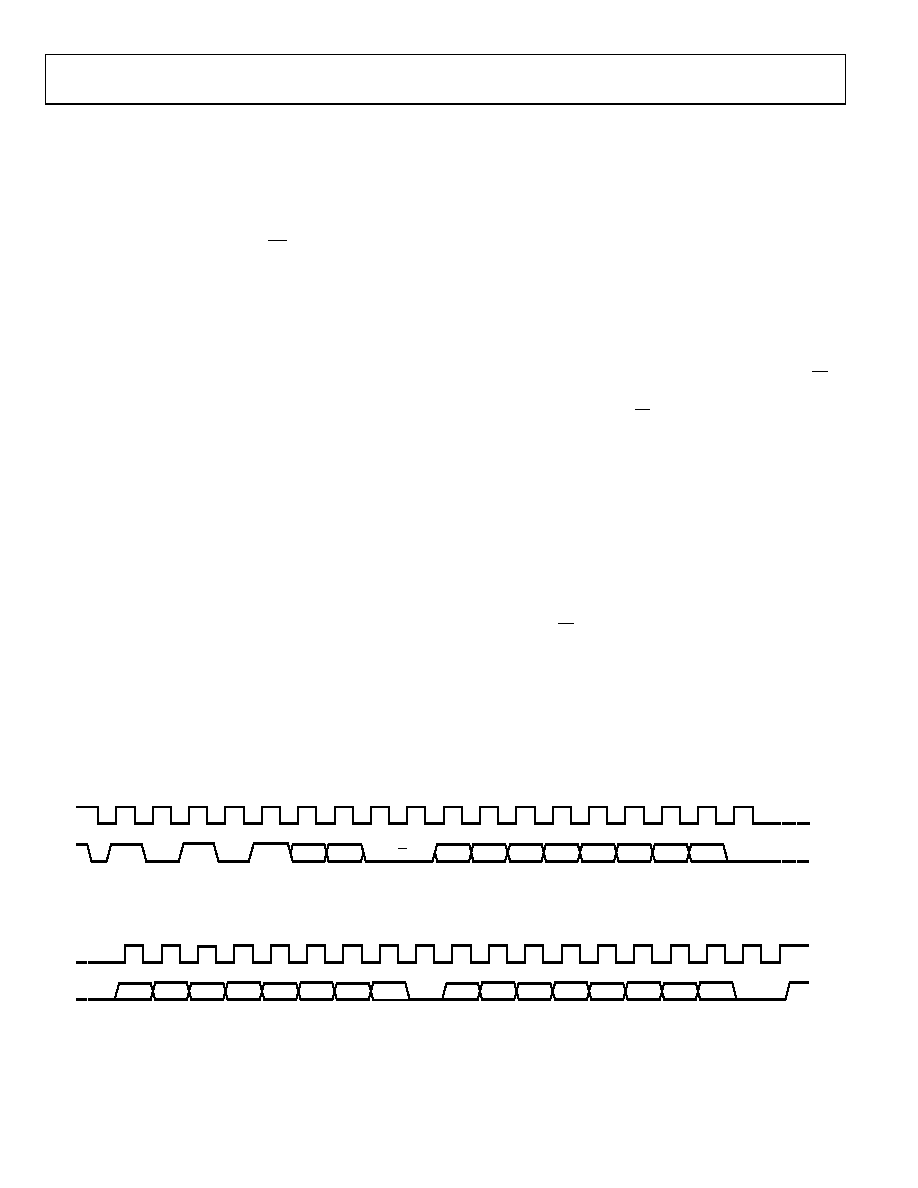
Write Operation
Data can be written to the AD5384 DACs in three modes: 4-byte
mode, 3-byte mode, and 2-byte mode.
4-Byte Mode
When writing to the AD5384 DACs, the user must begin with an
address byte (R/W = 0), after which the DAC acknowledges that it
is prepared to receive data by pulling SDA low. The address byte is
followed by the pointer byte; this addresses the specific channel in
the DAC to be addressed and also is acknowledged by the DAC.
Two bytes of data are then written to the DAC, as shown in
Figure 27. A stop condition follows. This lets the user update a
single channel within the AD5384 at any time, and requires four
bytes of data to transfer from the master.
1
0
1
0
1
AD1
AD0
R/W
0
A5
A4
A3
A2
A1
A0
SCL
SDA
SCL
SDA
START COND
BY MASTER
ACK BY
AD538x
ACK BY
AD538x
ADDRESS BYTE
MOST SIGNIFICANT BYTE
LEAST SIGNIFICANT BYTE
POINTER BYTE
MSB
ACK BY
AD538x
ACK BY
AD538x
STOP
COND
BY
MASTER
REG1
REG0
MSB
LSB
MSB
LSB
04652-
029
Figure 27. 4-Byte, I2C Write Operation
Rev. B | Page 26 of 32
相关PDF资料 |
PDF描述 |
|---|---|
| VE-J0H-MY-S | CONVERTER MOD DC/DC 52V 50W |
| VI-B42-IV-S | CONVERTER MOD DC/DC 15V 150W |
| VI-2WW-IW-S | CONVERTER MOD DC/DC 5.5V 100W |
| VE-JTL-MY-S | CONVERTER MOD DC/DC 28V 50W |
| VE-J0F-MY-S | CONVERTER MOD DC/DC 72V 50W |
相关代理商/技术参数 |
参数描述 |
|---|---|
| AD5384BBCZ-5 | 功能描述:IC DAC 14BIT 40CH 5V 100-CSPBGA RoHS:是 类别:集成电路 (IC) >> 数据采集 - 数模转换器 系列:- 标准包装:2,400 系列:- 设置时间:- 位数:18 数据接口:串行 转换器数目:3 电压电源:模拟和数字 功率耗散(最大):- 工作温度:-40°C ~ 85°C 安装类型:表面贴装 封装/外壳:36-TFBGA 供应商设备封装:36-TFBGA 包装:带卷 (TR) 输出数目和类型:* 采样率(每秒):* |
| AD5384BBCZ-5REEL7 | 功能描述:14 Bit Digital to Analog Converter 40 100-CSBGA (10x10) 制造商:analog devices inc. 系列:denseDAC 包装:带卷(TR) 零件状态:有效 位数:14 数模转换器数:40 建立时间:8μs 输出类型:Voltage - Buffered 差分输出:无 数据接口:I2C,SPI,DSP 参考类型:外部, 内部 电压 - 电源,模拟:5V 电压 - 电源,数字:2.7 V ~ 5.5 V INL/DNL(LSB):±4(最大),-1/+2(最大) 架构:电阻串 DAC 工作温度:-40°C ~ 85°C 封装/外壳:100-LFBGA,CSPBGA 供应商器件封装:100-CSBGA(10x10) 标准包装:400 |
| AD538AD | 功能描述:IC MULT/DIV REALTIME ACU 18-CDIP RoHS:否 类别:集成电路 (IC) >> 线性 - 模拟乘法器,除法器 系列:- 标准包装:25 系列:HA 功能:模拟乘法器 位元/级数:四象限 封装/外壳:16-CDIP(0.300",7.62mm) 供应商设备封装:16-CDIP 侧面铜焊 包装:管件 |
| AD538ADZ | 功能描述:IC REALTIME ACU UNIT 18-CDIP RoHS:是 类别:集成电路 (IC) >> 线性 - 模拟乘法器,除法器 系列:- 标准包装:25 系列:HA 功能:模拟乘法器 位元/级数:四象限 封装/外壳:16-CDIP(0.300",7.62mm) 供应商设备封装:16-CDIP 侧面铜焊 包装:管件 |
| AD538BD | 功能描述:IC MULT/DIV REALTIME ACU 18-CDIP RoHS:否 类别:集成电路 (IC) >> 线性 - 模拟乘法器,除法器 系列:- 标准包装:25 系列:HA 功能:模拟乘法器 位元/级数:四象限 封装/外壳:16-CDIP(0.300",7.62mm) 供应商设备封装:16-CDIP 侧面铜焊 包装:管件 |
发布紧急采购,3分钟左右您将得到回复。