参数资料
| 型号: | AD5390BSTZ-5 |
| 厂商: | Analog Devices Inc |
| 文件页数: | 32/44页 |
| 文件大小: | 0K |
| 描述: | IC DAC 14BIT I2C 16CH 52-LQFP |
| 产品培训模块: | Data Converter Fundamentals DAC Architectures |
| 产品变化通告: | AD5390/1/2 Redesign Change 16/May/2012 |
| 设计资源: | 8 to 16 Channels of Programmable Voltage with Excellent Temperature Drift Performance Using AD5390/1/2 (CN0029) AD5390/91/92 Channel Monitor Function (CN0030) |
| 标准包装: | 1 |
| 设置时间: | 8µs |
| 位数: | 14 |
| 数据接口: | I²C,串行 |
| 转换器数目: | 16 |
| 电压电源: | 单电源 |
| 功率耗散(最大): | 35mW |
| 工作温度: | -40°C ~ 85°C |
| 安装类型: | 表面贴装 |
| 封装/外壳: | 52-LQFP |
| 供应商设备封装: | 52-LQFP(10x10) |
| 包装: | 托盘 |
| 输出数目和类型: | 16 电压,单极 |
| 采样率(每秒): | 125k |
| 产品目录页面: | 782 (CN2011-ZH PDF) |
| 配用: | EVAL-AD5390EBZ-ND - BOARD EVALUATION FOR AD5390 |
第1页第2页第3页第4页第5页第6页第7页第8页第9页第10页第11页第12页第13页第14页第15页第16页第17页第18页第19页第20页第21页第22页第23页第24页第25页第26页第27页第28页第29页第30页第31页当前第32页第33页第34页第35页第36页第37页第38页第39页第40页第41页第42页第43页第44页
AD5390/AD5391/AD5392
Data Sheet
Rev. E | Page 38 of 44
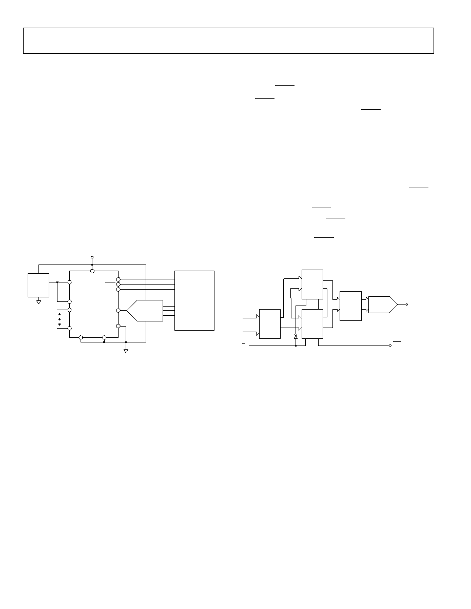
AD539x MONITOR FUNCTION
The AD5390 contains a channel monitor function consisting
of a multiplexer addressed via the interface, allowing any
channel output to be routed to this pin for monitoring using
an external ADC. The channel monitor function must be
enabled in the control register before any channels are routed
to the MON_OUT pin.
Table 23 and Table 24 contain the decoding information
required to route any channel on the AD5390, AD5391, and
AD5392 to the MON_OUT pin. Selecting Channel Address 63
three-states the MON_OUT pin. The AD539x family also
contains two monitor input pins called MON_IN 1 and
MON_IN 2. The user can connect external signals to these
pins, which under software control can be multiplexed to
MON_OUT for monitoring purposes. Figure 43 shows a typical
monitoring circuit implemented using a 12-bit SAR ADC in a
6-lead SOT package. The external reference input is connected
to MON_IN 1 to allow it to be easily monitored. The controller
output port selects the channel to be monitored, and the input
port reads the converted data from the ADC.
03773-
030
AD5390
AD780/
ADR431
AGND
MON_OUT
MON_IN1
SCLK
SYNC
DIN
REFOUT/REFIN
AVDD
OUTPUT PORT
INPUT PORT
CONTROLLER
VOUT 0
VOUT 15
AVDD
DAC_GND SIGNAL_GND
AD7476
CS
SCLK
SDATA
GND
VIN
Figure 43. Typical Channel Monitoring Circuit
TOGGLE MODE FUNCTION
The toggle mode function allows an output signal to be
generated using the LDAC control signal that switches between
two DAC data registers. This function is configured using the
SFR control register, as follows: A write with REG1 = REG0 = 0,
A3 to A0 = 1100 specifies a control register write. The toggle
mode function is enabled in groups of eight channels using Bit
CR3 and Bit CR2 in the AD5390/AD5392 control register and
using Bit CR1 and Bit CR0 in the AD5391 control register. (See
the Control Register Write section.) Figure 44 shows a block
diagram of the toggle mode implementation. Each DAC
channel on the AD539x contains an A and a B data register.
Note that the B registers can be loaded only when toggle mode
is enabled.
To configure the AD539x for toggle mode of operation, the
sequence of events is as follows:
1. Enable toggle mode for the required channels via the
control register.
2. Load data to all A registers.
3. Load data to all B registers.
4. Apply LDAC.
The LDAC is used to switch between the A and B registers in
determining the analog output. The first LDAC configures the
output to reflect the data in the A registers. This mode offers
significant advantages if the user wants to generate a square
wave at the output on all channels, as could be required to drive
a liquid-crystal-based, variable optical attenuator.
Configuring the AD5390, for example, the user writes to the
control register and sets CR3 = 1 and CR2 = 1, enabling the two
groups of eight for toggle mode operation. The user must then
load data to all 16 A registers and B registers. Toggling the LDAC
sets the output values to reflect the data in the A and B registers,
and the frequency of the LDAC determines the frequency of the
square wave output. The first LDAC loads the contents of the A
registers to the DAC registers. Toggle mode is disabled via the
control register; the first LDAC following the disabling of the
toggle mode updates the outputs with the data contained in the
A registers.
03773-
03
1
14-BIT DAC
VOUT
LDAC
CONTROL INPUT
DAC
REGISTER
INPUT
REGISTER
INPUT
DATA
REGISTER
A
DATA
REGISTER
B
A/B
Figure 44. Toggle Mode Function
THERMAL MONITOR FUNCTION
The AD539x family has a temperature shutdown function to
protect the chip in case multiple outputs are shorted. The short-
circuit current of each output amplifier is typically 40 mA.
Operating the AD539x at 5 V leads to a power dissipation of
200 mW/shorted amplifier. With five channels shorted, this
leads to an extra watt of power dissipation. For the 52-lead
LQFP, the θJA is typically 44°C/W.
The thermal monitor is enabled by the user using CR8 in the
AD5390/AD5392 control register and CR6 in the AD5391
control register. The output amplifiers on the AD539x are
automatically powered down if the die temperature exceeds
approximately 130°C. After a thermal shutdown has occurred,
the user can re-enable the part by executing a soft power-up if
the temperature has dropped below 130°C or by turning off the
thermal monitor function via the control register.
相关PDF资料 |
PDF描述 |
|---|---|
| VE-BNH-MU-S | CONVERTER MOD DC/DC 52V 200W |
| VE-JWX-MZ-B1 | CONVERTER MOD DC/DC 5.2V 25W |
| VE-BNF-MU-S | CONVERTER MOD DC/DC 72V 200W |
| VE-JWW-MZ-B1 | CONVERTER MOD DC/DC 5.5V 25W |
| VE-J1M-MZ-B1 | CONVERTER MINIMOD DC/DC 10V 25W |
相关代理商/技术参数 |
参数描述 |
|---|---|
| AD5391BCP | 制造商:Analog Devices 功能描述:DAC HEXADECIMAL RES-STRING 12-BIT 64LFCSP - Bulk |
| AD5391BCP-3 | 制造商:Analog Devices 功能描述:DAC 16-CH Resistor-String 12-bit 64-Pin LFCSP EP 制造商:Rochester Electronics LLC 功能描述:8/16-CHANNEL, 14/12-BIT, 3V/5V VOLTAGE OUT DAC - Bulk |
| AD5391BCP-3-REEL | 制造商:Analog Devices 功能描述:DAC 16-CH Resistor-String 12-bit 64-Pin LFCSP EP T/R |
| AD5391BCP-3-REEL7 | 制造商:Analog Devices 功能描述:DAC 16-CH Resistor-String 12-bit 64-Pin LFCSP EP T/R |
| AD5391BCP-5 | 制造商:Analog Devices 功能描述:DAC 16-CH Resistor-String 12-bit 64-Pin LFCSP EP 制造商:Analog Devices 功能描述:12BIT DAC 16CH 5V 5391 LFCSP-64 |
发布紧急采购,3分钟左右您将得到回复。