- 您现在的位置:买卖IC网 > PDF目录8751 > AD5424YRUZ-REEL (Analog Devices Inc)IC DAC 8BIT MULTIPLYING 16-TSSOP PDF资料下载
参数资料
| 型号: | AD5424YRUZ-REEL |
| 厂商: | Analog Devices Inc |
| 文件页数: | 11/29页 |
| 文件大小: | 0K |
| 描述: | IC DAC 8BIT MULTIPLYING 16-TSSOP |
| 产品培训模块: | Data Converter Fundamentals DAC Architectures |
| 标准包装: | 2,500 |
| 设置时间: | 30ns |
| 位数: | 8 |
| 数据接口: | 并联 |
| 转换器数目: | 1 |
| 电压电源: | 单电源 |
| 功率耗散(最大): | 25µW |
| 工作温度: | -40°C ~ 125°C |
| 安装类型: | 表面贴装 |
| 封装/外壳: | 16-TSSOP(0.173",4.40mm 宽) |
| 供应商设备封装: | 16-TSSOP |
| 包装: | 带卷 (TR) |
| 输出数目和类型: | 2 电流,单极;2 电流,双极 |
| 采样率(每秒): | 20.4M |
| 配用: | EVAL-AD5424EBZ-ND - BOARD EVALUATION FOR AD5424 |
第1页第2页第3页第4页第5页第6页第7页第8页第9页第10页当前第11页第12页第13页第14页第15页第16页第17页第18页第19页第20页第21页第22页第23页第24页第25页第26页第27页第28页第29页
AD5424/AD5433/AD5445
Data Sheet
Rev. D | Page 18 of 28
THEORY OF OPERATION
current output DACs consisting of a standard inverting R-2R
ladder configuration. A simplified diagram for the 8-bit AD5424 is
value of R. The value of R is typically 10 kΩ (minimum 8 kΩ
and maximum 12 kΩ). If IOUT1 and IOUT2 are kept at the same
potential, a constant current flows in each ladder leg, regardless
of digital input code. Therefore, the input resistance presented
at VREF is always constant and nominally of resistance value R.
The DAC output (IOUT) is code-dependent, producing various
resistances and capacitances. External amplifier choice should
take into account the variation in impedance generated by the
DAC on the amplifiers inverting input node.
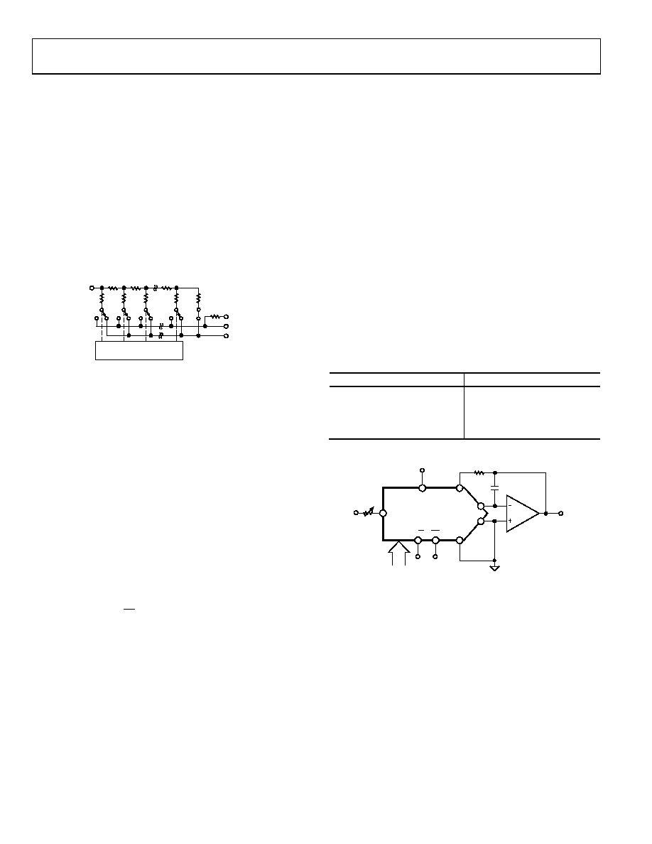
03160-048
VREF
RR
R
2R
S1
S2
S3
S8
2R
DAC DATA LATCHES
AND DRIVERS
RFBA
IOUT1
IOUT2
Figure 48. Simplified Ladder
Access is provided to the VREF, RFB, IOUT1, and IOUT2 terminals of
the DAC, making the device extremely versatile and allowing it
to be configured in several different operating modes, for example,
to provide a unipolar output, 4-quadrant multiplication in bipolar
mode or in single-supply modes of operation. Note that a matching
switch is used in series with the internal RFB feedback resistor. If
users attempt to measure RFB, power must be applied to VDD to
achieve continuity.
CIRCUIT OPERATION
Unipolar Mode
Using a single op amp, these devices can easily be configured to
provide 2-quadrant multiplying operation or a unipolar output
voltage swing, as shown in Figure 49.
When an output amplifier is connected in unipolar mode, the
output voltage is given by
n
REF
OUT
D
V
2
where D is the fractional representation of the digital word loaded
to the DAC and n is the resolution of the DAC.
D = 0 to 255 (8-bit AD5424)
= 0 to 1023 (10-bit AD5433)
= 0 to 4095 (12-bit AD5445)
Note that the output voltage polarity is opposite to the VREF
polarity for dc reference voltages.
These DACs are designed to operate with either negative or positive
reference voltages. The VDD power pin is only used by the internal
digital logic to drive the DAC switches’ on and off states.
These DACs are also designed to accommodate ac reference
input signals in the range of –10 V to +10 V.
With a fixed 10 V reference, the circuit shown in Figure 49 gives
a unipolar 0 V to –10 V output voltage swing. When VIN is an ac
signal, the circuit performs 2-quadrant multiplication.
Table 7 shows the relationship between digital code and expected
output voltage for unipolar operation (AD5424, 8-bit device).
Table 7. Unipolar Code Table
Digital Input
Analog Output (V)
1111 1111
–VREF (255/256)
1000 0000
–VREF (128/256) = –VREF/2
0000 0001
VREF (1/256)
0000 0000
VREF (0/256) = 0
03160-049
VREF
VDD
R/W
R1
R2
IOUT1
IOUT2
CS
RFB
GND
C1
A1
AGND
DATA
INPUTS
VOUT =
0 TO –VREF
R1 AND R2 USED ONLY IF GAIN ADJUSTMENT IS REQUIRED.
C1 PHASE COMPENSATION (1pF TO 2pF) MAY BE REQUIRED
IF A1 IS A HIGH SPEED AMPLIFIER.
NOTES:
1.
2.
AD5424/
AD5433/
AD5445
Figure 49. Unipolar Operation
相关PDF资料 |
PDF描述 |
|---|---|
| ICS8535AGI-01LF | IC CLOCK BUFFER MUX 2:4 20-TSSOP |
| VE-25W-MW-F3 | CONVERTER MOD DC/DC 5.5V 100W |
| VE-JNH-MZ-F1 | CONVERTER MOD DC/DC 52V 25W |
| VE-25W-MW-F2 | CONVERTER MOD DC/DC 5.5V 100W |
| VE-25W-MW-F1 | CONVERTER MOD DC/DC 5.5V 100W |
相关代理商/技术参数 |
参数描述 |
|---|---|
| AD5424YRUZ-REEL7 | 功能描述:IC DAC 8BIT MULTIPLYING 16-TSSOP RoHS:是 类别:集成电路 (IC) >> 数据采集 - 数模转换器 系列:- 产品培训模块:Data Converter Fundamentals DAC Architectures 设计资源:Unipolar, Precision DC Digital-to-Analog Conversion using AD5450/1/2/3 8-14-Bit DACs (CN0052) Precision, Bipolar, Configuration for AD5450/1/2/3 8-14bit Multiplying DACs (CN0053) AC Signal Processing Using AD5450/1/2/3 Current Output DACs (CN0054) Programmable Gain Element Using AD5450/1/2/3 Current Output DAC Family (CN0055) Single Supply Low Noise LED Current Source Driver Using a Current Output DAC in the Reverse Mode (CN0139) 标准包装:10,000 系列:- 设置时间:- 位数:12 数据接口:DSP,MICROWIRE?,QSPI?,串行,SPI? 转换器数目:1 电压电源:单电源 功率耗散(最大):- 工作温度:-40°C ~ 125°C 安装类型:表面贴装 封装/外壳:SOT-23-8 薄型,TSOT-23-8 供应商设备封装:TSOT-23-8 包装:带卷 (TR) 输出数目和类型:1 电流,单极;1 电流,双极 采样率(每秒):2.7M |
| AD5425 | 制造商:AD 制造商全称:Analog Devices 功能描述:8-Bit, High Bandwidth Multiplying DAC with Serial Interface |
| AD5425BRM | 制造商:Analog Devices 功能描述:DAC 1CH R-2R 8BIT 10PIN USOIC - Bulk |
| AD5425YRM | 功能描述:IC DAC MULTIPLYING 8BIT 10-MSOP RoHS:否 类别:集成电路 (IC) >> 数据采集 - 数模转换器 系列:- 产品培训模块:LTC263x 12-, 10-, and 8-Bit VOUT DAC Family 特色产品:LTC2636 - Octal 12-/10-/8-Bit SPI VOUT DACs with 10ppm/°C Reference 标准包装:91 系列:- 设置时间:4µs 位数:10 数据接口:MICROWIRE?,串行,SPI? 转换器数目:8 电压电源:单电源 功率耗散(最大):2.7mW 工作温度:-40°C ~ 85°C 安装类型:表面贴装 封装/外壳:14-WFDFN 裸露焊盘 供应商设备封装:14-DFN-EP(4x3) 包装:管件 输出数目和类型:8 电压,单极 采样率(每秒):* |
| AD5425YRM-REEL | 功能描述:IC DAC 8BIT MULTIPLYING 10-MSOP RoHS:否 类别:集成电路 (IC) >> 数据采集 - 数模转换器 系列:- 产品培训模块:Data Converter Fundamentals DAC Architectures 设计资源:Unipolar, Precision DC Digital-to-Analog Conversion using AD5450/1/2/3 8-14-Bit DACs (CN0052) Precision, Bipolar, Configuration for AD5450/1/2/3 8-14bit Multiplying DACs (CN0053) AC Signal Processing Using AD5450/1/2/3 Current Output DACs (CN0054) Programmable Gain Element Using AD5450/1/2/3 Current Output DAC Family (CN0055) Single Supply Low Noise LED Current Source Driver Using a Current Output DAC in the Reverse Mode (CN0139) 标准包装:10,000 系列:- 设置时间:- 位数:12 数据接口:DSP,MICROWIRE?,QSPI?,串行,SPI? 转换器数目:1 电压电源:单电源 功率耗散(最大):- 工作温度:-40°C ~ 125°C 安装类型:表面贴装 封装/外壳:SOT-23-8 薄型,TSOT-23-8 供应商设备封装:TSOT-23-8 包装:带卷 (TR) 输出数目和类型:1 电流,单极;1 电流,双极 采样率(每秒):2.7M |
发布紧急采购,3分钟左右您将得到回复。