参数资料
| 型号: | AD5441BRMZ |
| 厂商: | Analog Devices Inc |
| 文件页数: | 5/17页 |
| 文件大小: | 0K |
| 描述: | IC DAC 12BIT SERIAL IN 8MSOP |
| 产品培训模块: | Data Converter Fundamentals DAC Architectures |
| 标准包装: | 50 |
| 设置时间: | 500ns |
| 位数: | 12 |
| 数据接口: | 串行 |
| 转换器数目: | 1 |
| 电压电源: | 单电源 |
| 功率耗散(最大): | 55µW |
| 工作温度: | -40°C ~ 125°C |
| 安装类型: | 表面贴装 |
| 封装/外壳: | 8-TSSOP,8-MSOP(0.118",3.00mm 宽) |
| 供应商设备封装: | 8-MSOP |
| 包装: | 管件 |
| 输出数目和类型: | 1 电流,单极;1 电流,双极 |
| 采样率(每秒): | * |
| 产品目录页面: | 782 (CN2011-ZH PDF) |
| 配用: | EVAL-AD5541/42EBZ-ND - BOARD EVAL FOR AD5441/2 |
AD5441
Rev. A | Page 12 of 16
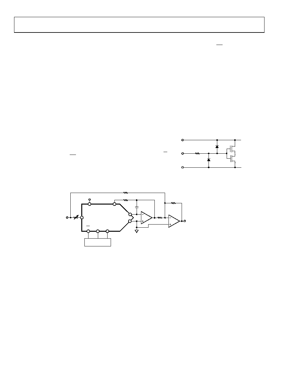
BIPOLAR 4-QUADRANT MULTIPLYING
Figure 24 shows a suggested circuit to achieve 4-quadrant
multiplying operation. The summing amplifier multiplies VOUT1
by 2 and offsets the output with the reference voltage so that a
midscale digital input code of 2048 places VOUT2 at 0 V. The negative
full-scale voltage is VREF when the DAC is loaded with all zeros.
The positive full-scale output is (VREF 1 LSB) when the DAC
is loaded with all ones. Therefore, the digital coding is offset
binary. The voltage output transfer equation for various input
data and reference (or signal) values follows
VOUT2 = (D/2048 1) VREF
where:
D is the decimal data loaded into the DAC register.
VREF is the externally applied reference voltage source.
INTERFACE LOGIC INFORMATION
The AD5441 has been designed for ease of operation. The
timing diagram in Figure 2 illustrates the input register loading
sequence. Note that the most significant bit (MSB) is loaded
first. Once the 12-bit input register is full, the data is transferred
to the DAC register by taking LD momentarily low.
DIGITAL SECTION
The digital inputs of the AD5441, SRI, LD, and CLK, are TTL-
compatible. The input voltage levels affect the amount of current
drawn from the supply; peak supply current occurs as the digital
input (VIN) passes through the transition region. See
for the supply current vs. logic input voltage graph. Maintaining
the digital input voltage levels as close as possible to the supplies,
VDD and GND, minimizes supply current consumption. The
digital inputs of the AD5441 were designed with ESD resistance
incorporated through careful layout and the inclusion of input
protection circuitry.
shows the input protection diodes
and series resistor; this input structure is duplicated on each
digital input. High voltage static charges applied to the inputs
are shunted to the supply and ground rails through forward-
biased diodes. These protection diodes were designed to clamp
the inputs to well below dangerous levels during static discharge
conditions.
VDD
LD, CLK, SRI
GND
5k
06
49
2-
0
2
0
Figure 23. Digital Input Protection
06
49
2-
0
24
NOTES
1. R1 AND R2 ARE USED ONLY IF GAIN ADJUSTMENT IS REQUIRED.
ADJUST R1 FOR VOUT = 0V WITH CODE 10000000 LOADED TO DAC.
2. MATCHING AND TRACKING IS ESSENTIAL FOR RESISTOR PAIRS
R3 AND R4.
3. C1 PHASE COMPENSATION (1pF TO 2pF) MAY BE REQUIRED
IF A1/A2 IS A HIGH SPEED AMPLIFIER.
RFB
IOUT1
GND
VREF
±10V
VREF
R1
AD5441
VDD
AGND
C1
A1
A2
R2
VOUT = –VREF TO +VREF
CONTROLLER
R3
20k
R4
10k
R5
20k
CLK
SRI
LD
Figure 24. Bipolar (4-Quadrant) Operation
相关PDF资料 |
PDF描述 |
|---|---|
| D38999/20SC4PC | CONN RCPT 4POS WALL MNT W/PINS |
| AD7302BNZ | IC DAC 8BIT DUAL R-R 20-DIP |
| AD5623RBRMZ-3 | IC DAC NANO 12BIT DUAL 10-MSOP |
| VE-BNX-MV-F1 | CONVERTER MOD DC/DC 5.2V 150W |
| VI-201-MY-F2 | CONVERTER MOD DC/DC 12V 50W |
相关代理商/技术参数 |
参数描述 |
|---|---|
| AD5441BRMZ-REEL7 | 功能描述:IC DAC 12BIT SERIAL IN 8MSOP RoHS:是 类别:集成电路 (IC) >> 数据采集 - 数模转换器 系列:- 产品培训模块:LTC263x 12-, 10-, and 8-Bit VOUT DAC Family 特色产品:LTC2636 - Octal 12-/10-/8-Bit SPI VOUT DACs with 10ppm/°C Reference 标准包装:91 系列:- 设置时间:4µs 位数:10 数据接口:MICROWIRE?,串行,SPI? 转换器数目:8 电压电源:单电源 功率耗散(最大):2.7mW 工作温度:-40°C ~ 85°C 安装类型:表面贴装 封装/外壳:14-WFDFN 裸露焊盘 供应商设备封装:14-DFN-EP(4x3) 包装:管件 输出数目和类型:8 电压,单极 采样率(每秒):* |
| AD5442ABCPZ-1 | 制造商:AD 制造商全称:Analog Devices 功能描述:2.7 V to 5.5 V, Serial-Input, Voltage-Output, 16-/12-Bit nanoDACs in LFCSP |
| AD5442JR | 制造商:Analog Devices 功能描述: |
| AD5443 | 制造商:AD 制造商全称:Analog Devices 功能描述:Dual 8-,10-,12-Bit High Bandwidth Multiplying DACs with Serial Interface |
| AD5443BRM | 制造商:Analog Devices 功能描述:DAC SGL R-2R 12-BIT 10PIN USOIC - Bulk |
发布紧急采购,3分钟左右您将得到回复。