- 您现在的位置:买卖IC网 > PDF目录8757 > AD5450YUJZ-REEL (Analog Devices Inc)IC DAC 8BIT MULTIPLYING TSOT23-8 PDF资料下载
参数资料
| 型号: | AD5450YUJZ-REEL |
| 厂商: | Analog Devices Inc |
| 文件页数: | 14/28页 |
| 文件大小: | 0K |
| 描述: | IC DAC 8BIT MULTIPLYING TSOT23-8 |
| 产品培训模块: | Data Converter Fundamentals DAC Architectures |
| 设计资源: | Unipolar, Precision DC Digital-to-Analog Conversion using AD5450/1/2/3 8-14-Bit DACs (CN0052) Precision, Bipolar, Configuration for AD5450/1/2/3 8-14bit Multiplying DACs (CN0053) AC Signal Processing Using AD5450/1/2/3 Current Output DACs (CN0054) Programmable Gain Element Using AD5450/1/2/3 Current Output DAC Family (CN0055) |
| 标准包装: | 10,000 |
| 位数: | 8 |
| 数据接口: | DSP,MICROWIRE?,QSPI?,串行,SPI? |
| 转换器数目: | 1 |
| 电压电源: | 单电源 |
| 工作温度: | -40°C ~ 125°C |
| 安装类型: | 表面贴装 |
| 封装/外壳: | SOT-23-8 薄型,TSOT-23-8 |
| 供应商设备封装: | TSOT-23-8 |
| 包装: | 带卷 (TR) |
| 输出数目和类型: | 1 电流,单极;1 电流,双极 |
| 采样率(每秒): | 2.7M |
第1页第2页第3页第4页第5页第6页第7页第8页第9页第10页第11页第12页第13页当前第14页第15页第16页第17页第18页第19页第20页第21页第22页第23页第24页第25页第26页第27页第28页
Data Sheet
AD5450/AD5451/AD5452/AD5453
Rev. G | Page 21 of 28
SERIAL INTERFACE
3-wire interface that is compatible with SPI, QSPI, MICROWIRE,
and most DSP interface standards. Data is written to the device in
16-bit words. This 16-bit word consists of two control bits and 8,
10, 12, or 14 data bits, as shown in Figure 50, Figure 51, Figure 52,
and Figure 53. The AD5453 uses all 14 bits of DAC data, the
10 bits and ignores the four LSBs, and the AD5450 uses 8 bits
and ignores the six LSBs.
DAC Control Bits C1, C0
Control Bits C1 and C0 allow the user to load and update the
new DAC code and to change the active clock edge. By default,
the shift register clocks data upon the falling edge; this can be
changed via the control bits. If changed, the DAC core is
inoperative until the next data frame, and a power recycle is
required to return it to active on the falling edge. A power cycle
resets the core to default condition. On-chip power-on reset
circuitry ensures that the device powers on with zero scale
loaded to the DAC register and IOUT line.
Table 10. DAC Control Bits
C1
C0
Function Implemented
0
Load and update (power-on default)
0
1
Reserved
1
0
Reserved
1
Clock data to shift register upon rising edge
SYNC Function
SYNC is an edge-triggered input that acts as a frame-
synchronization signal and chip enable. Data can only be
transferred to the device while SYNC is low. To start the serial
data transfer, SYNC should be taken low, observing the
minimum SYNC falling to SCLK falling edge setup time, t4. To
minimize the power consumption of the device, the interface
powers up fully only when the device is being written to, that is,
upon the falling edge of SYNC. The SCLK and SDIN input
buffers are powered down upon the rising edge of SYNC.
After the falling edge of the 16th SCLK pulse, bring SYNC high
to transfer data from the input shift register to the DAC register.
The serial interface to the AD5450 uses a 16-bit shift register.
Take care to avoid incomplete data sequences as these will be
latched to update the DAC output.
For example,
Loading 0x3FFF (a complete data sequence) will update
the output to 10 V (full scale).
User intends to write 0x3200 but after 12 active edges
SYNC goes high (incomplete write sequence). This will
actually update the following code: 0xF200.
The user expects an output of 5.6 V. However, if SYNC
goes high after 12 valid clock edges then an incomplete
data sequence of 12 bits is loaded. To complete the shift
register the 4 LSBs from the previous sequence are taken
and used as the 4 MSBs missing. The addition of these
4 bits will put the part in rising edge mode and the output
show the data frames for this example.
Also note that if more then 16-bits are loaded to the part before
SYNC goes high the last 16-bits will be latched.
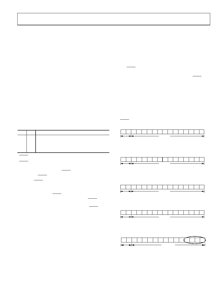
04587-005
DB0 (LSB)
DB15 (MSB)
C1
C0
X
DB7 DB6 DB5 DB4
DB3 DB2
DB0
DB1
CONTROL BITS
DATA BITS
Figure 50. AD5450 8-Bit Input Shift Register Contents
04587-006
DB0 (LSB)
DB15 (MSB)
DB5 DB4 DB3 DB2
DB0
DB1
C1
C0
DB7 DB6
DB8
DB9
X
CONTROL BITS
DATA BITS
Figure 51. AD5451 10-Bit Input Shift Register Contents
04587-007
DB0 (LSB)
DB15 (MSB)
DB7 DB6 DB5 DB4 DB3 DB2
DB0
DB1
C1
C0
DB11 DB10
DB8
DB9
X
CONTROL BITS
DATA BITS
Figure 52. AD5452 12-Bit Input Shift Register Contents
04587-008
DB0 (LSB)
DB15 (MSB)
DB9 DB8 DB7 DB6 DB5 DB4
DB2
DB3
C1
C0
DB13 DB12
DB10
DB11
DB0
DB1
CONTROL BITS
DATA BITS
Figure 53. AD5453 14-Bit Input Shift Register Contents
04587-
054
1
0
1
CONTROL BITS
DATA BITS
Figure 54. AD5453 First Write, Complete Data Sequence (0x3FFF)
相关PDF资料 |
PDF描述 |
|---|---|
| VI-JWB-MW | CONVERTER MOD DC/DC 95V 100W |
| VE-B4F-MV-F3 | CONVERTER MOD DC/DC 72V 150W |
| VE-B4D-MV-F1 | CONVERTER MOD DC/DC 85V 150W |
| VI-JW4-MW | CONVERTER MOD DC/DC 48V 100W |
| AD5301BRTZ-REEL7 | IC DAC 8BIT 2WIRE I2C SOT23-6 |
相关代理商/技术参数 |
参数描述 |
|---|---|
| AD5450YUJZ-REEL7 | 功能描述:IC DAC 8BIT MULT 50MHZ TSOT23-8 RoHS:是 类别:集成电路 (IC) >> 数据采集 - 数模转换器 系列:- 产品培训模块:Data Converter Fundamentals DAC Architectures 标准包装:3,000 系列:nanoDAC™ 设置时间:80µs 位数:18 数据接口:DSP,MICROWIRE?,QSPI?,串行,SPI? 转换器数目:1 电压电源:单电源 功率耗散(最大):- 工作温度:-40°C ~ 105°C 安装类型:表面贴装 封装/外壳:SOT-23-8 供应商设备封装:SOT-23-8 包装:带卷 (TR) 输出数目和类型:1 电压,单极 采样率(每秒):- 产品目录页面:784 (CN2011-ZH PDF) 配用:EVAL-AD5680EBZ-ND - BOARD EVAL FOR AD5680 其它名称:AD5680BRJZ-2REEL7TR |
| AD5451 | 制造商:AD 制造商全称:Analog Devices 功能描述:Dual 8-,10-,12-Bit High Bandwidth Multiplying DACs with Serial Interface |
| AD5451YUJ | 制造商:Analog Devices 功能描述:DAC 1CH R-2R 10-BIT 8PIN TSOT - Bulk |
| AD5451YUJ-REEL | 制造商:Analog Devices 功能描述:DAC 1-CH Segment 10-bit 8-Pin TSOT T/R |
| AD5451YUJ-REEL7 | 制造商:Analog Devices 功能描述:DAC 1-CH Segment 10-bit 8-Pin TSOT T/R 制造商:Rochester Electronics LLC 功能描述: |
发布紧急采购,3分钟左右您将得到回复。