- 您现在的位置:买卖IC网 > PDF目录8757 > AD5450YUJZ-REEL (Analog Devices Inc)IC DAC 8BIT MULTIPLYING TSOT23-8 PDF资料下载
参数资料
| 型号: | AD5450YUJZ-REEL |
| 厂商: | Analog Devices Inc |
| 文件页数: | 17/28页 |
| 文件大小: | 0K |
| 描述: | IC DAC 8BIT MULTIPLYING TSOT23-8 |
| 产品培训模块: | Data Converter Fundamentals DAC Architectures |
| 设计资源: | Unipolar, Precision DC Digital-to-Analog Conversion using AD5450/1/2/3 8-14-Bit DACs (CN0052) Precision, Bipolar, Configuration for AD5450/1/2/3 8-14bit Multiplying DACs (CN0053) AC Signal Processing Using AD5450/1/2/3 Current Output DACs (CN0054) Programmable Gain Element Using AD5450/1/2/3 Current Output DAC Family (CN0055) |
| 标准包装: | 10,000 |
| 位数: | 8 |
| 数据接口: | DSP,MICROWIRE?,QSPI?,串行,SPI? |
| 转换器数目: | 1 |
| 电压电源: | 单电源 |
| 工作温度: | -40°C ~ 125°C |
| 安装类型: | 表面贴装 |
| 封装/外壳: | SOT-23-8 薄型,TSOT-23-8 |
| 供应商设备封装: | TSOT-23-8 |
| 包装: | 带卷 (TR) |
| 输出数目和类型: | 1 电流,单极;1 电流,双极 |
| 采样率(每秒): | 2.7M |
第1页第2页第3页第4页第5页第6页第7页第8页第9页第10页第11页第12页第13页第14页第15页第16页当前第17页第18页第19页第20页第21页第22页第23页第24页第25页第26页第27页第28页
AD5450/AD5451/AD5452/AD5453
Data Sheet
Rev. G | Page 24 of 28
MICROWIRE-to-AD5450/AD5451/AD5452/AD5453
Interface
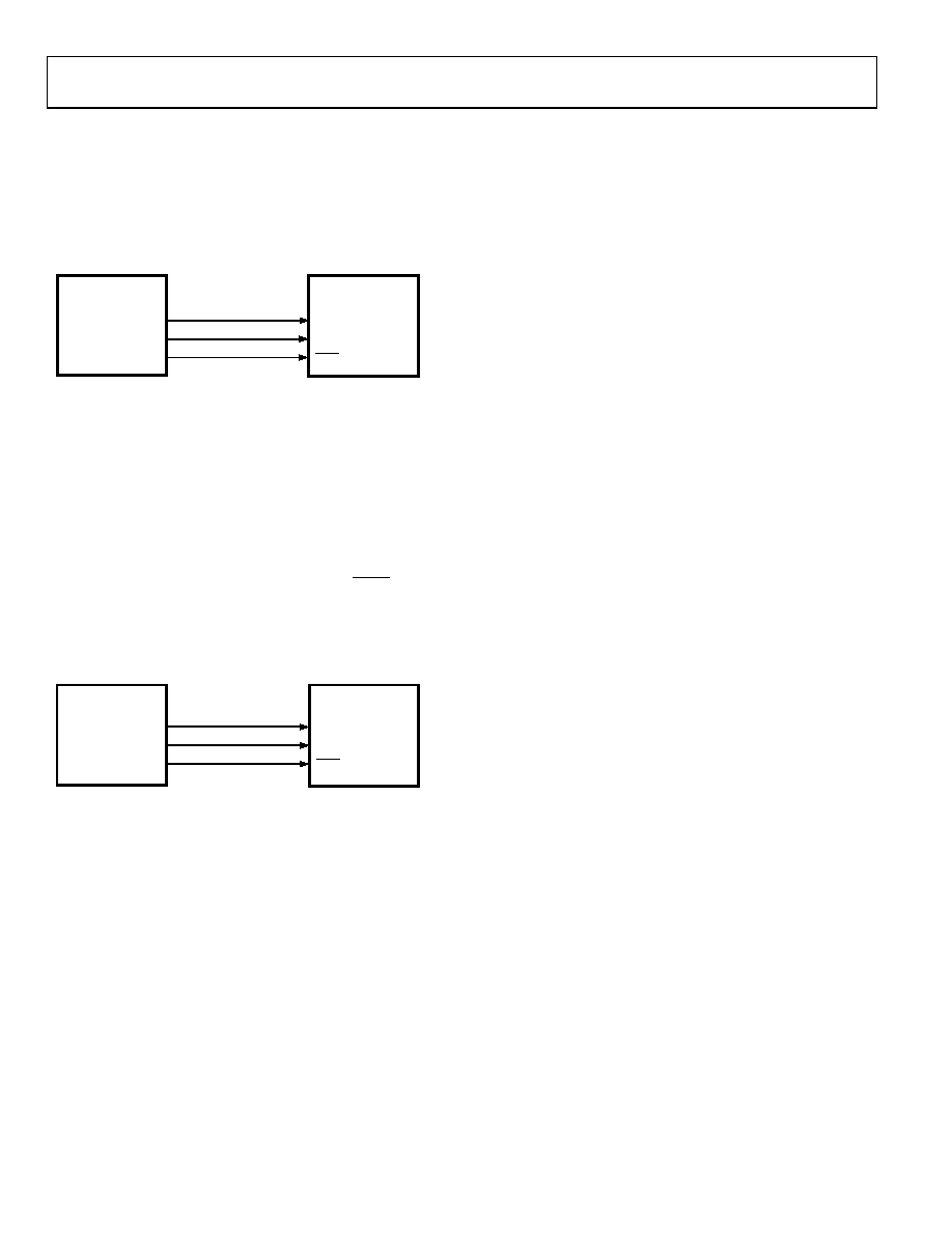
Figure 62 shows an interface between the DAC and any
MICROWIRE-compatible device. Serial data is shifted out
upon the falling edge of the serial clock, SK, and is clocked into
the DAC input shift register upon the rising edge of SK, which
corresponds to the falling edge of the DAC’s SCLK.
SCLK
SK
MICROWIRE*
SYNC
CS
SDIN
SO
AD5450/AD5451/
AD5452/AD5453*
*ADDITIONAL PINS OMITTED FOR CLARITY
04587-106
PIC16C6x/PIC16C7x-to-
AD5450/AD5451/AD5452/AD5453 Interface
The PIC16C6x/PIC16C7x synchronous serial port (SSP) is
configured as an SPI master with the clock polarity bit (CKP) = 0.
This is done by writing to the synchronous serial port control
register (SSPCON); see the PIC16/PIC17 Microcontroller
User Manual.
In this example, I/O Port RA1 is used to provide a SYNC signal
and enable the serial port of the DAC. This microcontroller
transfers only eight bits of data during each serial transfer
operation; therefore, two consecutive write operations are
required. Figure 63 shows the connection diagram.
SCLK
SCK/RC3
PIC16C6x/PIC16C7x*
SYNC
RA1
SDIN
SDI/RC4
AD5450/AD5451/
AD5452/AD5453*
*ADDITIONAL PINS OMITTED FOR CLARITY
04587-
107
PCB LAYOUT AND POWER SUPPLY DECOUPLING
In any circuit where accuracy is important, careful consideration
of the power supply and ground return layout helps to ensure
the rated performance. The printed circuit board on which a
designed so that the analog and digital sections are separated
and confined to certain areas of the board. If the DAC is in a
system where multiple devices require an AGND-to-DGND
connection, the connection should be made at one point only.
The star ground point should be established as close as possible
to the device.
These DACs should have ample supply bypassing of 10 F in
parallel with 0.1 F on the supply located as close to the package
as possible, ideally right up against the device. The 0.1 F
capacitor should have low effective series resistance (ESR) and
low effective series inductance (ESI), like the common ceramic
types that provide a low impedance path to ground at high
frequencies, to handle transient currents due to internal logic
switching. Low ESR 1 F to 10 F tantalum or electrolytic
capacitors should also be applied at the supplies to minimize
transient disturbance and filter out low frequency ripple.
Components, such as clocks, that produce fast switching signals
should be shielded with a digital ground to avoid radiating noise
to other parts of the board, and they should never be run near
the reference inputs.
Avoid crossover of digital and analog signals. Traces on opposite
sides of the board should run at right angles to each other. This
reduces the effects of feedthrough through the board. A microstrip
technique is the best solution, but its use is not always possible
with a double-sided board. In this technique, the component
side of the board is dedicated to the ground plane and signal
traces are placed on the solder side.
It is good practice to employ compact, minimum lead length
PCB layout design. Leads to the input should be as short as
possible to minimize IR drops and stray inductance.
The PCB metal traces between VREF and RFB should also be
matched to minimize gain error. To optimize high frequency
performance, the I-to-V amplifier should be located as close to
the device as possible.
相关PDF资料 |
PDF描述 |
|---|---|
| VI-JWB-MW | CONVERTER MOD DC/DC 95V 100W |
| VE-B4F-MV-F3 | CONVERTER MOD DC/DC 72V 150W |
| VE-B4D-MV-F1 | CONVERTER MOD DC/DC 85V 150W |
| VI-JW4-MW | CONVERTER MOD DC/DC 48V 100W |
| AD5301BRTZ-REEL7 | IC DAC 8BIT 2WIRE I2C SOT23-6 |
相关代理商/技术参数 |
参数描述 |
|---|---|
| AD5450YUJZ-REEL7 | 功能描述:IC DAC 8BIT MULT 50MHZ TSOT23-8 RoHS:是 类别:集成电路 (IC) >> 数据采集 - 数模转换器 系列:- 产品培训模块:Data Converter Fundamentals DAC Architectures 标准包装:3,000 系列:nanoDAC™ 设置时间:80µs 位数:18 数据接口:DSP,MICROWIRE?,QSPI?,串行,SPI? 转换器数目:1 电压电源:单电源 功率耗散(最大):- 工作温度:-40°C ~ 105°C 安装类型:表面贴装 封装/外壳:SOT-23-8 供应商设备封装:SOT-23-8 包装:带卷 (TR) 输出数目和类型:1 电压,单极 采样率(每秒):- 产品目录页面:784 (CN2011-ZH PDF) 配用:EVAL-AD5680EBZ-ND - BOARD EVAL FOR AD5680 其它名称:AD5680BRJZ-2REEL7TR |
| AD5451 | 制造商:AD 制造商全称:Analog Devices 功能描述:Dual 8-,10-,12-Bit High Bandwidth Multiplying DACs with Serial Interface |
| AD5451YUJ | 制造商:Analog Devices 功能描述:DAC 1CH R-2R 10-BIT 8PIN TSOT - Bulk |
| AD5451YUJ-REEL | 制造商:Analog Devices 功能描述:DAC 1-CH Segment 10-bit 8-Pin TSOT T/R |
| AD5451YUJ-REEL7 | 制造商:Analog Devices 功能描述:DAC 1-CH Segment 10-bit 8-Pin TSOT T/R 制造商:Rochester Electronics LLC 功能描述: |
发布紧急采购,3分钟左右您将得到回复。