参数资料
| 型号: | AD549KH |
| 厂商: | Analog Devices Inc |
| 文件页数: | 2/20页 |
| 文件大小: | 0K |
| 描述: | IC OPAMP GP 1MHZ LP 20MA TO99-8 |
| 标准包装: | 1 |
| 系列: | Topgate™ |
| 放大器类型: | 通用 |
| 电路数: | 1 |
| 转换速率: | 3 V/µs |
| 增益带宽积: | 1MHz |
| 电流 - 输入偏压: | 0.075pA |
| 电压 - 输入偏移: | 150µV |
| 电流 - 电源: | 600µA |
| 电流 - 输出 / 通道: | 20mA |
| 电压 - 电源,单路/双路(±): | ±5 V ~ 18 V |
| 工作温度: | 0°C ~ 70°C |
| 安装类型: | 通孔 |
| 封装/外壳: | TO-99-8 金属罐 |
| 供应商设备封装: | TO-99-8 |
| 包装: | 散装 |
AD549
Rev. H | Page 10 of 20
FUNCTIONAL DESCRIPTION
MINIMIZING INPUT CURRENT
The AD549 is optimized for low input current and offset
voltage. Careful attention to how the amplifier is used reduces
input currents in actual applications.
Keep the amplifier operating temperature as low as possible to
minimize input current. Like other JFET input amplifiers, the
AD549 input current is sensitive to chip temperature, rising by
a factor of 2.3 for every 10°C. Figure 25 is a plot of the AD549
input current vs. ambient temperature.
1nA
100pA
10pA
1pA
100fA
10fA
1fA
–55
–25
5
35
65
125
95
00
51
1-
0
25
TEMPERATURE (°C)
INP
U
T
BI
AS
CU
RRE
N
T
Figure 25. Input Bias Current vs. Ambient Temperature
On-chip power dissipation raises the chip operating tempera-
ture, causing an increase in input bias current. Due to the low
quiescent supply current of the AD549, the chip temperature
is less than 3°C higher than its ambient temperature when the
(unloaded) amplifier is operating with 15 V supplies. The
difference in the input current is negligible.
However, heavy output loads can cause a significant increase in
chip temperature and a corresponding increase in the input
current. Maintaining a minimum load resistance of 10 Ω is
recommended. Input current vs. additional power dissipation
due to output drive current is plotted in Figure 26.
6
5
4
3
2
1
0
25
50
75
100
125
150
175
200
00
51
1-
0
26
ADDITIONAL INTERNAL POWER DISSIPATION (mW)
NO
RM
AL
IZ
E
D
I
NP
UT
B
IA
S
CURR
E
NT
BASED ON
TYPICAL IB = 40fA
Figure 26. Input Bias Current vs. Additional Power Dissipation
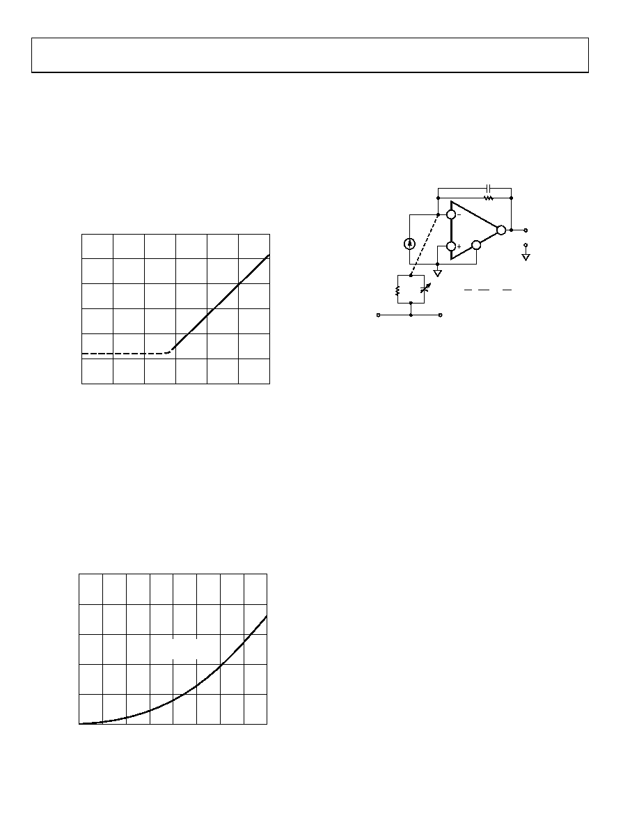
CIRCUIT BOARD NOTES
A number of physical phenomena generate spurious currents
that degrade the accuracy of low current measurements. Figure 27
is a schematic of a current to voltage (I-to-V) converter with
these parasitic currents modeled.
00
51
1-
02
7
2
3
6
8
AD549
+
VOUT
–
fS
CF
RF
VS
RP
CP
II' =
+V +
CP
V
RP
dCP
dT
dV
dT
Figure 27. Sources of Parasitic Leakage Currents
Finite resistance from input lines to voltages on the board,
modeled by Resistor RP, results in parasitic leakage. Insulation
resistance of more than 1015 Ω must be maintained between
the amplifier signal and supply lines to capitalize on the low
input currents of the AD549. Standard PCB material does not
have high enough insulation resistance; therefore, connect the
input leads of the AD549 to standoffs made of insulating
material with adequate volume resistivity (that is, Teflon). The
surface of the insulator must be kept clean to preserve surface
resistivity. For Teflon, an effective cleaning procedure consists
of swabbing the surface with high grade isopropyl alcohol,
rinsing with deionized water, and baking the board at 80°C for
10 minutes.
In addition to high volume and surface resistivity, other proper-
ties are desirable in the insulating material chosen. Resistance
to water absorption is important because surface water films
drastically reduce surface resistivity. The insulator chosen
should also exhibit minimal piezoelectric effects (charge
emission due to mechanical stress) and triboelectric effects
(charge generated by friction). Charge imbalances generated
by these mechanisms can appear as parasitic leakage currents.
These effects are modeled by Variable Capacitor CP in Figure 27.
Guarding the input lines by completely surrounding them with
a metal conductor biased near the potential of the input lines
has two major benefits. First, parasitic leakage from the signal
line is reduced because the voltage between the input line and
the guard is very low. Second, stray capacitance at the input
node is minimized. Input capacitance can substantially degrade
signal bandwidth and the stability of the I-to-V converter.
1 Electronic Measurements, pp. 15–17, Keithley Instruments, Inc., Cleveland,
Ohio, 1977.
相关PDF资料 |
PDF描述 |
|---|---|
| AD524BD | IC AMP INST 1MHZ PREC LN 16CDIP |
| TV02W480-G | TVS 200W 48V UNIDIRECT SOD-123 |
| TV02W450-HF | TVS 200W 45V UNIDIRECT SOD-123 |
| TV02W450-G | TVS 200W 45V UNIDIRECT SOD-123 |
| TV02W430-HF | TVS 200W 43V UNIDIRECT SOD-123 |
相关代理商/技术参数 |
参数描述 |
|---|---|
| AD549KH/+ | 制造商:未知厂家 制造商全称:未知厂家 功能描述:Voltage-Feedback Operational Amplifier |
| AD549KHZ | 功能描述:IC OPAMP GP 1MHZ LP 20MA TO99-8 RoHS:是 类别:集成电路 (IC) >> Linear - Amplifiers - Instrumentation 系列:Topgate™ 标准包装:2,500 系列:- 放大器类型:通用 电路数:4 输出类型:- 转换速率:0.6 V/µs 增益带宽积:1MHz -3db带宽:- 电流 - 输入偏压:45nA 电压 - 输入偏移:2000µV 电流 - 电源:1.4mA 电流 - 输出 / 通道:40mA 电压 - 电源,单路/双路(±):3 V ~ 32 V,±1.5 V ~ 16 V 工作温度:0°C ~ 70°C 安装类型:表面贴装 封装/外壳:14-TSSOP(0.173",4.40mm 宽) 供应商设备封装:14-TSSOP 包装:带卷 (TR) 其它名称:LM324ADTBR2G-NDLM324ADTBR2GOSTR |
| AD549L | 制造商:AD 制造商全称:Analog Devices 功能描述:Ultralow Input Bias Current Operational Amplifier |
| AD549LH | 功能描述:IC OPAMP GP 1MHZ LP 20MA TO99-8 RoHS:否 类别:集成电路 (IC) >> Linear - Amplifiers - Instrumentation 系列:Topgate™ 标准包装:50 系列:- 放大器类型:J-FET 电路数:2 输出类型:- 转换速率:3.5 V/µs 增益带宽积:1MHz -3db带宽:- 电流 - 输入偏压:30pA 电压 - 输入偏移:2000µV 电流 - 电源:200µA 电流 - 输出 / 通道:- 电压 - 电源,单路/双路(±):7 V ~ 36 V,±3.5 V ~ 18 V 工作温度:0°C ~ 70°C 安装类型:通孔 封装/外壳:8-DIP(0.300",7.62mm) 供应商设备封装:8-PDIP 包装:管件 |
| AD549LH | 制造商:Analog Devices 功能描述:OP AMP U-LOW BIAS TO-99-8 549 |
发布紧急采购,3分钟左右您将得到回复。