参数资料
| 型号: | AD549KH |
| 厂商: | Analog Devices Inc |
| 文件页数: | 3/20页 |
| 文件大小: | 0K |
| 描述: | IC OPAMP GP 1MHZ LP 20MA TO99-8 |
| 标准包装: | 1 |
| 系列: | Topgate™ |
| 放大器类型: | 通用 |
| 电路数: | 1 |
| 转换速率: | 3 V/µs |
| 增益带宽积: | 1MHz |
| 电流 - 输入偏压: | 0.075pA |
| 电压 - 输入偏移: | 150µV |
| 电流 - 电源: | 600µA |
| 电流 - 输出 / 通道: | 20mA |
| 电压 - 电源,单路/双路(±): | ±5 V ~ 18 V |
| 工作温度: | 0°C ~ 70°C |
| 安装类型: | 通孔 |
| 封装/外壳: | TO-99-8 金属罐 |
| 供应商设备封装: | TO-99-8 |
| 包装: | 散装 |
AD549
Rev. H | Page 11 of 20
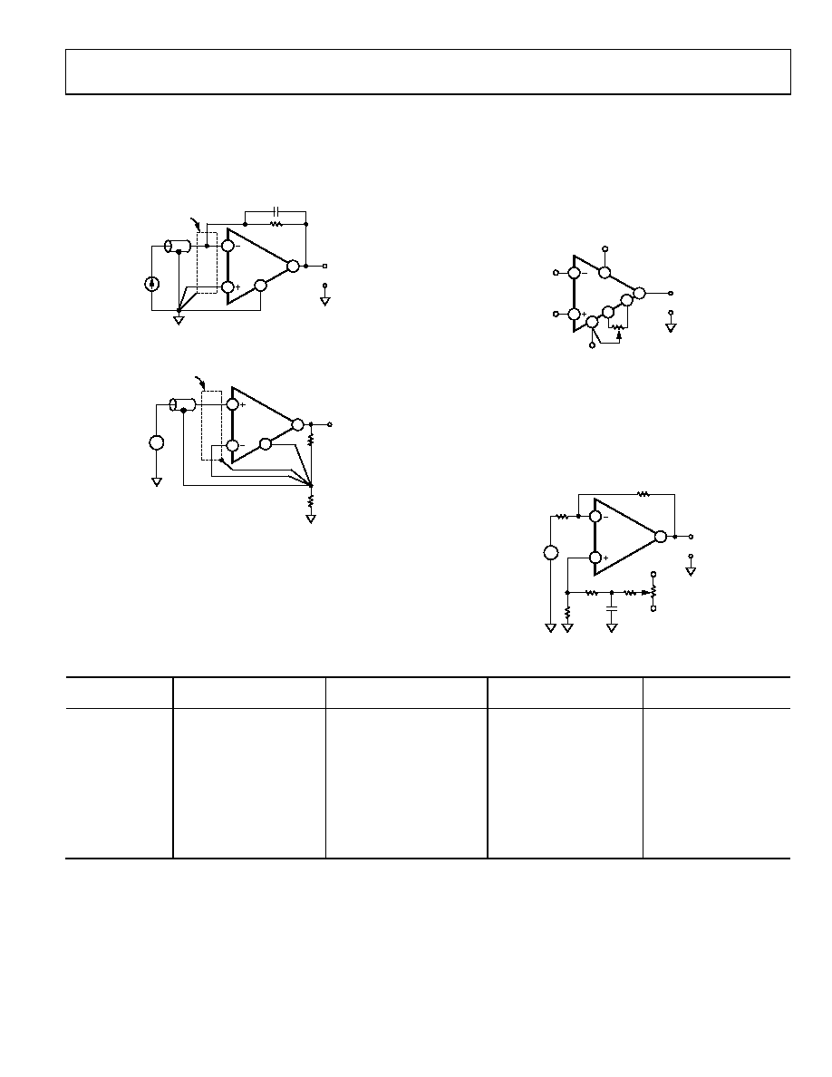
The case of the AD549 is connected to Pin 8 so that it can be
bootstrapped near the input potential. This minimizes pin
leakage and input common-mode capacitance due to the case.
Guard schemes for inverting and noninverting amplifier
00
51
1
-02
8
2
3
6
8
AD549
+
VOUT
–
IN
CF
RF
GUARD
Figure 28. Inverting Amplifier with Guard
0
05
11
-0
29
3
2
6
8
AD549
+
VOUT
–
VS
+
–
GUARD
RF
RI
Figure 29. Noninverting Amplifier with Guard
Other guidelines include keeping the circuit layout as compact
as possible and keeping the input lines short. Keeping the assembly
rigid and minimizing sources of vibration reduces triboelectric
and piezoelectric effects. All precision, high impedance circuitry
requires shielding against interference noise. Use low noise coaxial
or triaxial cables for remote connections to the input signal lines.
OFFSET NULLING
The AD549 input offset voltage can be nulled by using balance
Pin 1 and Pin 5, as shown in Figure 30. Nulling the input offset
voltage in this fashion introduces an added input offset voltage
drift component of 2.4 μV/°C per mV of nulled offset (a maxi-
mum additional drift of 0.6 μV/°C for the AD549K, 1.2 μV/°C
for the AD549L, and 2.4 μV/°C for the AD549J).
00
51
1-
03
0
2
3
6
5
1
7
4
AD549
+
VOUT
–
–VS
+VS
10k
Figure 30. Standard Offset Null Circuit
The approach in Figure 31 can be used when the amplifier is
used as an inverter. This method introduces a small voltage
referenced to the power supplies in series with the positive
input terminal of the amplifier. The amplifier input offset
voltage drift with temperature is not affected. However,
variation of the power supply voltages causes offset shifts.
0
05
1
1-
03
1
2
3
6
AD549
+
VOUT
–
VI
+
–
RF
RI
200
100k
499k
0.1F
–VS
+VS
Figure 31. Alternate Offset Null Circuit for Inverter
Table 3. Insulating Materials and Characteristics
Material
Volume Resistivity
(V to CM)
Minimal
Triboelectric Effect1
Minimal
Piezoelectric Effect1
Resistance to
Water Absorption1
Teflon
1017 to 1018
W
G
Kel-F
1017 to 1018
W
M
G
Sapphire
1016 to 1018
M
G
Polyethylene
1014 to 1018
M
G
M
Polystyrene
1012 to 1018
W
M
Ceramic
1012 to 1014
W
M
W
Glass Epoxy
1010 to 1017
W
M
W
PVC
1010 to 1015
G
M
G
Phenolic
105 to 1012
W
G
W
1 G: good with regard to property; M: moderate with regard to property; W: weak with regard to property.
相关PDF资料 |
PDF描述 |
|---|---|
| AD524BD | IC AMP INST 1MHZ PREC LN 16CDIP |
| TV02W480-G | TVS 200W 48V UNIDIRECT SOD-123 |
| TV02W450-HF | TVS 200W 45V UNIDIRECT SOD-123 |
| TV02W450-G | TVS 200W 45V UNIDIRECT SOD-123 |
| TV02W430-HF | TVS 200W 43V UNIDIRECT SOD-123 |
相关代理商/技术参数 |
参数描述 |
|---|---|
| AD549KH/+ | 制造商:未知厂家 制造商全称:未知厂家 功能描述:Voltage-Feedback Operational Amplifier |
| AD549KHZ | 功能描述:IC OPAMP GP 1MHZ LP 20MA TO99-8 RoHS:是 类别:集成电路 (IC) >> Linear - Amplifiers - Instrumentation 系列:Topgate™ 标准包装:2,500 系列:- 放大器类型:通用 电路数:4 输出类型:- 转换速率:0.6 V/µs 增益带宽积:1MHz -3db带宽:- 电流 - 输入偏压:45nA 电压 - 输入偏移:2000µV 电流 - 电源:1.4mA 电流 - 输出 / 通道:40mA 电压 - 电源,单路/双路(±):3 V ~ 32 V,±1.5 V ~ 16 V 工作温度:0°C ~ 70°C 安装类型:表面贴装 封装/外壳:14-TSSOP(0.173",4.40mm 宽) 供应商设备封装:14-TSSOP 包装:带卷 (TR) 其它名称:LM324ADTBR2G-NDLM324ADTBR2GOSTR |
| AD549L | 制造商:AD 制造商全称:Analog Devices 功能描述:Ultralow Input Bias Current Operational Amplifier |
| AD549LH | 功能描述:IC OPAMP GP 1MHZ LP 20MA TO99-8 RoHS:否 类别:集成电路 (IC) >> Linear - Amplifiers - Instrumentation 系列:Topgate™ 标准包装:50 系列:- 放大器类型:J-FET 电路数:2 输出类型:- 转换速率:3.5 V/µs 增益带宽积:1MHz -3db带宽:- 电流 - 输入偏压:30pA 电压 - 输入偏移:2000µV 电流 - 电源:200µA 电流 - 输出 / 通道:- 电压 - 电源,单路/双路(±):7 V ~ 36 V,±3.5 V ~ 18 V 工作温度:0°C ~ 70°C 安装类型:通孔 封装/外壳:8-DIP(0.300",7.62mm) 供应商设备封装:8-PDIP 包装:管件 |
| AD549LH | 制造商:Analog Devices 功能描述:OP AMP U-LOW BIAS TO-99-8 549 |
发布紧急采购,3分钟左右您将得到回复。