参数资料
| 型号: | AD549KH |
| 厂商: | Analog Devices Inc |
| 文件页数: | 5/20页 |
| 文件大小: | 0K |
| 描述: | IC OPAMP GP 1MHZ LP 20MA TO99-8 |
| 标准包装: | 1 |
| 系列: | Topgate™ |
| 放大器类型: | 通用 |
| 电路数: | 1 |
| 转换速率: | 3 V/µs |
| 增益带宽积: | 1MHz |
| 电流 - 输入偏压: | 0.075pA |
| 电压 - 输入偏移: | 150µV |
| 电流 - 电源: | 600µA |
| 电流 - 输出 / 通道: | 20mA |
| 电压 - 电源,单路/双路(±): | ±5 V ~ 18 V |
| 工作温度: | 0°C ~ 70°C |
| 安装类型: | 通孔 |
| 封装/外壳: | TO-99-8 金属罐 |
| 供应商设备封装: | TO-99-8 |
| 包装: | 散装 |
AD549
Rev. H | Page 13 of 20
00
51
1-
03
8
3
2
6
AD549
SOURCE
RPROTECT
DIFFERENTIAL INPUT VOLTAGE OVERLOAD
A plot of the AD549 input currents vs. differential input
input current at either terminal stays below a few hundred
femtoamps until one input terminal is forced higher than 1 V
to 1.5 V above the other terminal. Under these conditions, the
input current limits at 30 μA.
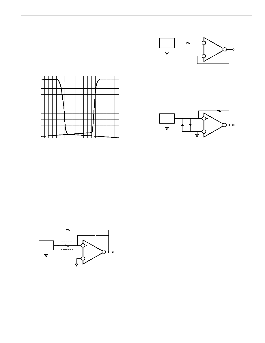
Figure 38. Follower with Input Current Limit
Figure 39 is a schematic of the AD549 as an inverter with an
input voltage clamp. Bootstrapping the clamp diodes at the
inverting input minimizes the voltage across the clamps and
keeps the leakage due to the diodes low. Use low leakage diodes,
such as the FD333s, and shield them from light to prevent photo-
currents from being generated. Even with these precautions, the
diodes measurably increase input current and capacitance.
100
10
1
100n
10n
1n
100p
10p
1p
100f
10f
–5
–4
–3
–2
–1
0
1
2
3
4
5
00
51
1-
03
6
DIFFERENTIAL INPUT VOLTAGE (V) (VIN+ – VIN–)
INP
UT
CURR
E
NT
(A)
IIN–IIN+
0
05
11
-03
9
2
3
6
AD549
SOURCE
RF
PROTECT
DIODES
Figure 39. Input Voltage Clamp with Diodes
SAMPLE-AND-DIFFERENCE CIRCUIT TO MEASURE
ELECTROMETER LEAKAGE CURRENTS
Figure 36. Input Current vs. Differential Input Voltage
INPUT PROTECTION
There are a number of methods used to test electrometer leakage
currents, including current integration and direct I-to-V con-
version. Regardless of the method used, board and interconnect
cleanliness, proper choice of insulating materials (such as Teflon
or Kel-F), correct guarding and shielding techniques, and care
in physical layout are essential to making accurate leakage
measurements.
The AD549 safely handles any input voltage within the supply
voltage range. Subjecting the input terminals to voltages beyond
the power supply can destroy the device or cause shifts in input
current or offset voltage if the amplifier is not protected.
A protection scheme for the amplifier as an inverter is shown
inverting input to 1 mA for expected transient (less than 1 sec)
overvoltage conditions, or to 100 μA for a continuous overload.
Because RP is inside the feedback loop and is much lower in
value than the amplifier input resistance, it does not affect the
dc gain of the inverter. However, the Johnson noise of the
resistor adds root sum of squares to the amplifier input noise.
Figure 40 is a schematic of the sample-and-difference circuit. It
uses two AD549 electrometer amplifiers (A and B) as I-to-V
converters with high value (1010 Ω) sense resistors (RSa and
RSb). R1 and R2 provide for an overall circuit sensitivity of
10 fA/mV (10 pA full scale). CC and CF provide noise suppression
and loop compensation. CC should be a low leakage polystyrene
capacitor. An ultralow leakage Kel-F test socket is used for con-
tacting the device under test. Rigid Teflon coaxial cable is used
to make connections to all high impedance nodes. The use of
rigid coaxial cable affords immunity to error induced by mechan-
ical vibration and provides an outer conductor for shielding. The
entire circuit is enclosed in a grounded metal box.
00
51
1-
03
7
2
3
6
AD549
CF
SOURCE
RPROTECT
RF
Figure 37. Inverter with Input Current Limit
In the corresponding version of this scheme for a follower,
terminal produce a pole in the signal frequency response at a
f = πRC. Again, the Johnson noise, RP, adds to the input
voltage noise of the amplifier.
相关PDF资料 |
PDF描述 |
|---|---|
| AD524BD | IC AMP INST 1MHZ PREC LN 16CDIP |
| TV02W480-G | TVS 200W 48V UNIDIRECT SOD-123 |
| TV02W450-HF | TVS 200W 45V UNIDIRECT SOD-123 |
| TV02W450-G | TVS 200W 45V UNIDIRECT SOD-123 |
| TV02W430-HF | TVS 200W 43V UNIDIRECT SOD-123 |
相关代理商/技术参数 |
参数描述 |
|---|---|
| AD549KH/+ | 制造商:未知厂家 制造商全称:未知厂家 功能描述:Voltage-Feedback Operational Amplifier |
| AD549KHZ | 功能描述:IC OPAMP GP 1MHZ LP 20MA TO99-8 RoHS:是 类别:集成电路 (IC) >> Linear - Amplifiers - Instrumentation 系列:Topgate™ 标准包装:2,500 系列:- 放大器类型:通用 电路数:4 输出类型:- 转换速率:0.6 V/µs 增益带宽积:1MHz -3db带宽:- 电流 - 输入偏压:45nA 电压 - 输入偏移:2000µV 电流 - 电源:1.4mA 电流 - 输出 / 通道:40mA 电压 - 电源,单路/双路(±):3 V ~ 32 V,±1.5 V ~ 16 V 工作温度:0°C ~ 70°C 安装类型:表面贴装 封装/外壳:14-TSSOP(0.173",4.40mm 宽) 供应商设备封装:14-TSSOP 包装:带卷 (TR) 其它名称:LM324ADTBR2G-NDLM324ADTBR2GOSTR |
| AD549L | 制造商:AD 制造商全称:Analog Devices 功能描述:Ultralow Input Bias Current Operational Amplifier |
| AD549LH | 功能描述:IC OPAMP GP 1MHZ LP 20MA TO99-8 RoHS:否 类别:集成电路 (IC) >> Linear - Amplifiers - Instrumentation 系列:Topgate™ 标准包装:50 系列:- 放大器类型:J-FET 电路数:2 输出类型:- 转换速率:3.5 V/µs 增益带宽积:1MHz -3db带宽:- 电流 - 输入偏压:30pA 电压 - 输入偏移:2000µV 电流 - 电源:200µA 电流 - 输出 / 通道:- 电压 - 电源,单路/双路(±):7 V ~ 36 V,±3.5 V ~ 18 V 工作温度:0°C ~ 70°C 安装类型:通孔 封装/外壳:8-DIP(0.300",7.62mm) 供应商设备封装:8-PDIP 包装:管件 |
| AD549LH | 制造商:Analog Devices 功能描述:OP AMP U-LOW BIAS TO-99-8 549 |
发布紧急采购,3分钟左右您将得到回复。