参数资料
| 型号: | AD5532ABC-2 |
| 厂商: | Analog Devices Inc |
| 文件页数: | 10/20页 |
| 文件大小: | 0K |
| 描述: | IC DAC 14BIT 32CH 74-CSPBGA |
| 产品培训模块: | Data Converter Fundamentals DAC Architectures |
| 标准包装: | 1 |
| 设置时间: | 30µs |
| 位数: | 14 |
| 数据接口: | 串行 |
| 转换器数目: | 34 |
| 电压电源: | 模拟和数字 |
| 功率耗散(最大): | 623mW |
| 工作温度: | -40°C ~ 85°C |
| 安装类型: | 表面贴装 |
| 封装/外壳: | 74-LBGA,CSPBGA |
| 供应商设备封装: | 74-CSPBGA(12x12) |
| 包装: | 托盘 |
| 输出数目和类型: | 32 电压,单极 |
| 采样率(每秒): | 45k |
| 配用: | EVAL-AD5532HSEBZ-ND - BOARD EVAL FOR AD5532HS EVAL-AD5532EBZ-ND - BOARD EVAL FOR AD5532 |
AD5532
Rev. D | Page 18 of 20
AD5532 to PIC16C6x/7x
The PIC16C6x/7x synchronous serial port (SSP) is configured
as an SPI master with the Clock Polarity Bit = 0. This is done by
writing to the synchronous serial port control register
(SSPCON). See the PIC16/17 Microcontroller User Manual. In
this example, the I/O port RA1 is being used to pulse SYNC
and enable the serial port of the AD5532. This microcontroller
transfers only eight bits of data during each serial transfer
operation; therefore, two or three consecutive read/write
operations are needed depending on the mode.
shows the connection diagram.
00939-C-023
AD5532*
*ADDITIONAL PINS OMITTED FOR CLARITY
PIC16C6x/7x*
SCLK
SCK/RC3
DOUT
SDO/RC5
DIN
SDI/RC4
RA1
SYNC
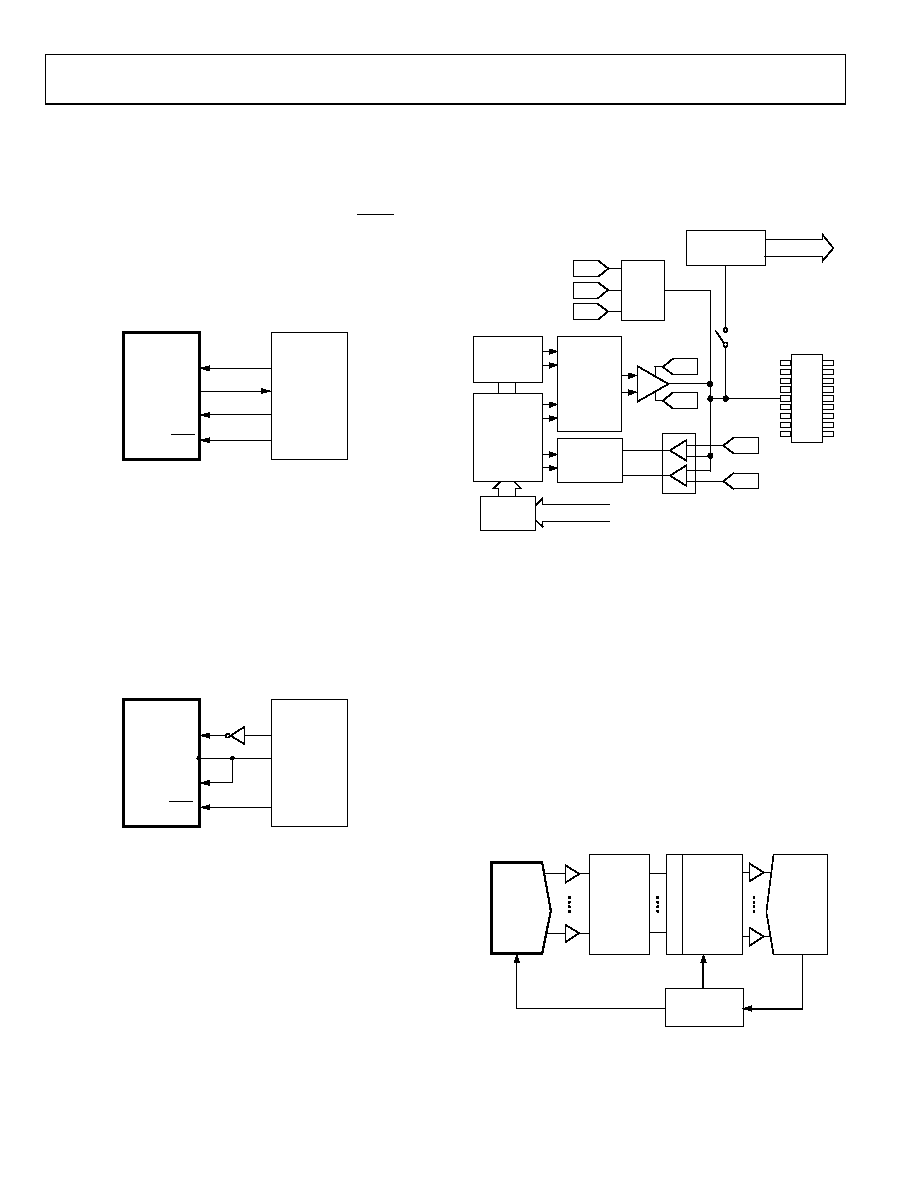
Figure 24. AD5532 to PIC16C6x/7x Interface
AD5532 to 8051
The AD5532 requires a clock synchronized to the serial data.
The 8051 serial interface must therefore be operated in Mode 0.
In this mode, serial data enters and exits through RxD and a
shift clock is output on TxD. Figure 25 shows how the 8051 is
connected to the AD5532. Because the AD5532 shifts data out
on the rising edge of the shift clock and latches data in on the
falling edge, the shift clock must be inverted. The AD5532
requires its data with the MSB first. Because the 8051 outputs
the LSB first, the transmit routine must take this into account.
00939-C-024
AD5532*
*ADDITIONAL PINS OMITTED FOR CLARITY
8051*
SCLK
TxD
DOUT
RxD
DIN
P1.1
SYNC
Figure 25. AD5532 to 8051 Interface
APPLICATION CIRCUITS
AD5532 in a Typical ATE System
The AD5532 is ideally suited for use in automatic test
equipment. Several DACs are required to control pin drivers,
comparators, active loads, and signal timing. Traditionally,
sample-and-hold devices were used in this application.
The AD5532 has several advantages: no refreshing is required,
there is no droop, pedestal error is eliminated, and there is no
need for extra filtering to remove glitches. Overall a higher level
of integration is achieved in a smaller area (see Figure 26).
00939-C-025
DACs
ACTIVE
LOAD
PARAMETRIC
MEASUREMENT
UNIT
DRIVER
COMPARATOR
COMPARE
REGISTER
STORED
DATA
AND INHIBIT
PATTERN
PERIOD
GENERATION
AND
DELAY
TIMING
FORMATTER
SYSTEM BUS
DAC
SYSTEM BUS
DUT
DAC
Figure 26. AD5532 in an ATE System
Typical Application Circuit (DAC Mode)
The AD5532 can be used in many optical networking
applications that require a large number of DACs to perform
control and measurement functions. In the example shown in
Figure 27, the outputs of the AD5532 are amplified and used to
control actuators that determine the position of MEMS mirrors
in an optical switch. The exact position of each mirror is
measured using sensors. The sensor readings are muxed using
four dual, 4-channel matrix switches (ADG739) and fed back to
an 8-channel, 14-bit ADC (AD7856).
The control loop is driven by an ADSP-2191M, a 16-bit fixed-
point DSP with 3 SPORT interfaces and 2 SPI ports. The DSP
uses some of these serial ports to write data to the DAC, control
the multiplexer, and read back data from the ADC.
00939-C-026
ADSP-2191M
AD5532
ADG739
×4
AD8544
×2
AD7856
1
32
1
32
1
8
MEMS
MIRROR
ARRAY
S
E
N
S
O
R
Figure 27. Typical Optical Control and Measurement Application Circuit
相关PDF资料 |
PDF描述 |
|---|---|
| AD5532ABC-1 | IC DAC 14BIT 32CH 74-CSPBGA |
| AD664JNZ-UNI | IC DAC 12BIT QUAD UNIPOL 28DIP |
| AD5370BSTZ-REEL | IC DAC 16BIT 40CH SERIAL 64-LQFP |
| AD5370BCPZ-REEL7 | IC DAC 16BIT 40CH SERIAL 64LFCSP |
| VE-J5P-MW-S | CONVERTER MOD DC/DC 13.8V 100W |
相关代理商/技术参数 |
参数描述 |
|---|---|
| AD5532ABC-3 | 功能描述:IC DAC 14BIT 32CH 74-CSPBGA RoHS:否 类别:集成电路 (IC) >> 数据采集 - 数模转换器 系列:- 产品培训模块:Lead (SnPb) Finish for COTS Obsolescence Mitigation Program 标准包装:1,000 系列:- 设置时间:1µs 位数:8 数据接口:串行 转换器数目:8 电压电源:双 ± 功率耗散(最大):941mW 工作温度:0°C ~ 70°C 安装类型:表面贴装 封装/外壳:24-SOIC(0.295",7.50mm 宽) 供应商设备封装:24-SOIC W 包装:带卷 (TR) 输出数目和类型:8 电压,单极 采样率(每秒):* |
| AD5532ABC-5 | 功能描述:IC DAC 14BIT 32CH 74-CSPBGA RoHS:否 类别:集成电路 (IC) >> 数据采集 - 数模转换器 系列:- 产品培训模块:Lead (SnPb) Finish for COTS Obsolescence Mitigation Program 标准包装:1,000 系列:- 设置时间:1µs 位数:8 数据接口:串行 转换器数目:8 电压电源:双 ± 功率耗散(最大):941mW 工作温度:0°C ~ 70°C 安装类型:表面贴装 封装/外壳:24-SOIC(0.295",7.50mm 宽) 供应商设备封装:24-SOIC W 包装:带卷 (TR) 输出数目和类型:8 电压,单极 采样率(每秒):* |
| AD5532ABCZ-1 | 功能描述:IC DAC 14BIT VOUT 32CH 74-CSPBGA RoHS:是 类别:集成电路 (IC) >> 数据采集 - 数模转换器 系列:- 标准包装:1 系列:- 设置时间:4.5µs 位数:12 数据接口:串行,SPI? 转换器数目:1 电压电源:单电源 功率耗散(最大):- 工作温度:-40°C ~ 125°C 安装类型:表面贴装 封装/外壳:8-SOIC(0.154",3.90mm 宽) 供应商设备封装:8-SOICN 包装:剪切带 (CT) 输出数目和类型:1 电压,单极;1 电压,双极 采样率(每秒):* 其它名称:MCP4921T-E/SNCTMCP4921T-E/SNRCTMCP4921T-E/SNRCT-ND |
| AD5532ABCZ-1REEL | 功能描述:IC DAC 14BIT 32CH BIPO 74-CSPBGA RoHS:是 类别:集成电路 (IC) >> 数据采集 - 数模转换器 系列:- 产品培训模块:Lead (SnPb) Finish for COTS Obsolescence Mitigation Program 标准包装:1,000 系列:- 设置时间:1µs 位数:8 数据接口:串行 转换器数目:8 电压电源:双 ± 功率耗散(最大):941mW 工作温度:0°C ~ 70°C 安装类型:表面贴装 封装/外壳:24-SOIC(0.295",7.50mm 宽) 供应商设备封装:24-SOIC W 包装:带卷 (TR) 输出数目和类型:8 电压,单极 采样率(每秒):* |
| AD5532ABCZ-2 | 功能描述:IC DAC 14BIT 32CH BIPO 74-CSPBGA RoHS:是 类别:集成电路 (IC) >> 数据采集 - 数模转换器 系列:- 产品培训模块:Lead (SnPb) Finish for COTS Obsolescence Mitigation Program 标准包装:1,000 系列:- 设置时间:1µs 位数:8 数据接口:串行 转换器数目:8 电压电源:双 ± 功率耗散(最大):941mW 工作温度:0°C ~ 70°C 安装类型:表面贴装 封装/外壳:24-SOIC(0.295",7.50mm 宽) 供应商设备封装:24-SOIC W 包装:带卷 (TR) 输出数目和类型:8 电压,单极 采样率(每秒):* |
发布紧急采购,3分钟左右您将得到回复。