参数资料
| 型号: | AD5532ABC-2 |
| 厂商: | Analog Devices Inc |
| 文件页数: | 9/20页 |
| 文件大小: | 0K |
| 描述: | IC DAC 14BIT 32CH 74-CSPBGA |
| 产品培训模块: | Data Converter Fundamentals DAC Architectures |
| 标准包装: | 1 |
| 设置时间: | 30µs |
| 位数: | 14 |
| 数据接口: | 串行 |
| 转换器数目: | 34 |
| 电压电源: | 模拟和数字 |
| 功率耗散(最大): | 623mW |
| 工作温度: | -40°C ~ 85°C |
| 安装类型: | 表面贴装 |
| 封装/外壳: | 74-LBGA,CSPBGA |
| 供应商设备封装: | 74-CSPBGA(12x12) |
| 包装: | 托盘 |
| 输出数目和类型: | 32 电压,单极 |
| 采样率(每秒): | 45k |
| 配用: | EVAL-AD5532HSEBZ-ND - BOARD EVAL FOR AD5532HS EVAL-AD5532EBZ-ND - BOARD EVAL FOR AD5532 |
AD5532
Rev. D | Page 17 of 20
PARALLEL INTERFACE (ISHA MODE ONLY)
The SER/PAR bit must be tied low to enable the parallel
interface and disable the serial interface. The parallel interface is
controlled by nine pins, as described in
.
Table 11.
Pin
Description
CS
Active low package select pin. This pin is shared
with the SYNC function for the serial interface.
WR
Active low write pin. The values on the address
pins are latched on a rising edge of WR.
A4–A0
Five address pins (A4 = MSB of address,
A0 = LSB). These are used to address the
relevant channel (out of a possible 32).
OFFSET_SEL
Offset select pin. This has the same function as
the Offset_Sel bit in the serial interface. When it
is high, the offset channel is addressed. The
address on A4–A0 is ignored in this case.
CAL
When this pin is high, all 32 channels acquire
VIN simultaneously. The acquisition time is then
45 μs (typ) and accuracy may be reduced.
MICROPROCESSOR INTERFACING
AD5532 to ADSP-21xx Interface
ADSP-21xx DSPs are easily interfaced to the AD5532 without
the need for extra logic.
A data transfer is initiated by writing a word to the TX register
after the SPORT has been enabled. In a write sequence, data is
clocked out on each rising edge of the DSP serial clock and
clocked into the AD5532 on the falling edge of its SCLK. In
readback, 16 bits of data are clocked out of the AD5532 on each
rising edge of SCLK and clocked into the DSP on the rising
edge of SCLK. DIN is ignored. The valid 14 bits of data is
centered in the 16-bit RX register in this configuration. The
SPORT Control register should be set up as in Table 12.
Table 12.
TFSW = RFSW = 1
Alternate framing
INVRFS = INVTFS = 1
Active low frame signal
DTYPE = 00
Right justify data
ISCLK = 1
Internal serial clock
TFSR = RFSR = 1
Frame every word
IRFS = 0
External framing signal
ITFS = 1
Internal framing signal
SLEN = 1001
10-bit data-words (ISHA mode write)
SLEN = 0111
3 × 8-bit data-words (DAC mode write)
SLEN = 1111
16-bit data-words (Readback mode)
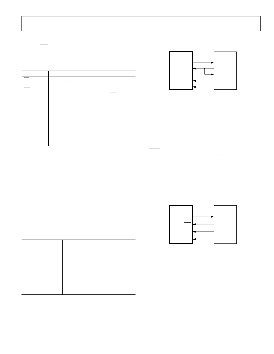
Figure 22 shows the connection diagram.
00939-C-021
DOUT
AD5532*
*ADDITIONAL PINS OMITTED FOR CLARITY
SYNC
DIN
SCLK
DR
TFS
DT
RFS
SCLK
ADSP-2101/
ADSP-2103*
Figure 22. AD5532 to ADSP-2101/ADSP-2103 Interface
AD5532 to MC68HC11
The serial peripheral interface (SPI) on the MC68HC11 is
configured for master mode (MSTR) = 1, clock polarity bit
(CPOL) = 0, and the clock phase bit (CPHA) = 1. The SPI is
configured by writing to the SPI control register (SPCR)—see
the 68HC11 User Manual. SCK of the 68HC11 drives the SCLK
of the AD5532, the MOSI output drives the serial data line (DIN)
of the AD5532, and the MISO input is driven from DOUT. The
SYNC signal is derived from a port line (PC7). When data is
being transmitted to the AD5532, the SYNC line is taken low
(PC7). Data appearing on the MOSI output is valid on the
falling edge of SCK. Serial data from the 68HC11 is transmitted
in 8-bit bytes with only eight falling clock edges occurring in
the transmit cycle. Data is transmitted MSB first. To transmit
10 data bits in ISHA mode, it is important to left-justify the data
in the SPDR register. PC7 must be pulled low to start a transfer.
It is taken high and pulled low again before other read/write
cycles can take place.
shows a connection diagram.
00939-C-022
AD5532*
*ADDITIONAL PINS OMITTED FOR CLARITY
MC68HC11*
DOUT
MISO
DIN
MOSI
SCLK
SCK
PC7
SYNC
Figure 23. AD5532 to MC68HC11 Interface
相关PDF资料 |
PDF描述 |
|---|---|
| AD5532ABC-1 | IC DAC 14BIT 32CH 74-CSPBGA |
| AD664JNZ-UNI | IC DAC 12BIT QUAD UNIPOL 28DIP |
| AD5370BSTZ-REEL | IC DAC 16BIT 40CH SERIAL 64-LQFP |
| AD5370BCPZ-REEL7 | IC DAC 16BIT 40CH SERIAL 64LFCSP |
| VE-J5P-MW-S | CONVERTER MOD DC/DC 13.8V 100W |
相关代理商/技术参数 |
参数描述 |
|---|---|
| AD5532ABC-3 | 功能描述:IC DAC 14BIT 32CH 74-CSPBGA RoHS:否 类别:集成电路 (IC) >> 数据采集 - 数模转换器 系列:- 产品培训模块:Lead (SnPb) Finish for COTS Obsolescence Mitigation Program 标准包装:1,000 系列:- 设置时间:1µs 位数:8 数据接口:串行 转换器数目:8 电压电源:双 ± 功率耗散(最大):941mW 工作温度:0°C ~ 70°C 安装类型:表面贴装 封装/外壳:24-SOIC(0.295",7.50mm 宽) 供应商设备封装:24-SOIC W 包装:带卷 (TR) 输出数目和类型:8 电压,单极 采样率(每秒):* |
| AD5532ABC-5 | 功能描述:IC DAC 14BIT 32CH 74-CSPBGA RoHS:否 类别:集成电路 (IC) >> 数据采集 - 数模转换器 系列:- 产品培训模块:Lead (SnPb) Finish for COTS Obsolescence Mitigation Program 标准包装:1,000 系列:- 设置时间:1µs 位数:8 数据接口:串行 转换器数目:8 电压电源:双 ± 功率耗散(最大):941mW 工作温度:0°C ~ 70°C 安装类型:表面贴装 封装/外壳:24-SOIC(0.295",7.50mm 宽) 供应商设备封装:24-SOIC W 包装:带卷 (TR) 输出数目和类型:8 电压,单极 采样率(每秒):* |
| AD5532ABCZ-1 | 功能描述:IC DAC 14BIT VOUT 32CH 74-CSPBGA RoHS:是 类别:集成电路 (IC) >> 数据采集 - 数模转换器 系列:- 标准包装:1 系列:- 设置时间:4.5µs 位数:12 数据接口:串行,SPI? 转换器数目:1 电压电源:单电源 功率耗散(最大):- 工作温度:-40°C ~ 125°C 安装类型:表面贴装 封装/外壳:8-SOIC(0.154",3.90mm 宽) 供应商设备封装:8-SOICN 包装:剪切带 (CT) 输出数目和类型:1 电压,单极;1 电压,双极 采样率(每秒):* 其它名称:MCP4921T-E/SNCTMCP4921T-E/SNRCTMCP4921T-E/SNRCT-ND |
| AD5532ABCZ-1REEL | 功能描述:IC DAC 14BIT 32CH BIPO 74-CSPBGA RoHS:是 类别:集成电路 (IC) >> 数据采集 - 数模转换器 系列:- 产品培训模块:Lead (SnPb) Finish for COTS Obsolescence Mitigation Program 标准包装:1,000 系列:- 设置时间:1µs 位数:8 数据接口:串行 转换器数目:8 电压电源:双 ± 功率耗散(最大):941mW 工作温度:0°C ~ 70°C 安装类型:表面贴装 封装/外壳:24-SOIC(0.295",7.50mm 宽) 供应商设备封装:24-SOIC W 包装:带卷 (TR) 输出数目和类型:8 电压,单极 采样率(每秒):* |
| AD5532ABCZ-2 | 功能描述:IC DAC 14BIT 32CH BIPO 74-CSPBGA RoHS:是 类别:集成电路 (IC) >> 数据采集 - 数模转换器 系列:- 产品培训模块:Lead (SnPb) Finish for COTS Obsolescence Mitigation Program 标准包装:1,000 系列:- 设置时间:1µs 位数:8 数据接口:串行 转换器数目:8 电压电源:双 ± 功率耗散(最大):941mW 工作温度:0°C ~ 70°C 安装类型:表面贴装 封装/外壳:24-SOIC(0.295",7.50mm 宽) 供应商设备封装:24-SOIC W 包装:带卷 (TR) 输出数目和类型:8 电压,单极 采样率(每秒):* |
发布紧急采购,3分钟左右您将得到回复。