参数资料
| 型号: | AD5532ABC-2 |
| 厂商: | Analog Devices Inc |
| 文件页数: | 6/20页 |
| 文件大小: | 0K |
| 描述: | IC DAC 14BIT 32CH 74-CSPBGA |
| 产品培训模块: | Data Converter Fundamentals DAC Architectures |
| 标准包装: | 1 |
| 设置时间: | 30µs |
| 位数: | 14 |
| 数据接口: | 串行 |
| 转换器数目: | 34 |
| 电压电源: | 模拟和数字 |
| 功率耗散(最大): | 623mW |
| 工作温度: | -40°C ~ 85°C |
| 安装类型: | 表面贴装 |
| 封装/外壳: | 74-LBGA,CSPBGA |
| 供应商设备封装: | 74-CSPBGA(12x12) |
| 包装: | 托盘 |
| 输出数目和类型: | 32 电压,单极 |
| 采样率(每秒): | 45k |
| 配用: | EVAL-AD5532HSEBZ-ND - BOARD EVAL FOR AD5532HS EVAL-AD5532EBZ-ND - BOARD EVAL FOR AD5532 |
AD5532
Rev. D | Page 14 of 20
FUNCTIONAL DESCRIPTION
The AD5532 consists of 32 DACs and an ADC (for ISHA
mode) in a single package. In DAC mode, a 14-bit digital word
is loaded into one of the 32 DAC Registers via the serial
interface. This is then converted (with gain and offset) into an
analog output voltage (VOUT0–VOUT31).
To update a DAC’s output voltage, the required DAC is
addressed via the serial port. When the DAC address and code
have been loaded, the selected DAC converts the code.
At power-on, all the DACs, including the offset channel, are
loaded with zeros. Each of the 33 DACs is offset internally by
50 mV (typ) from GND, so the outputs VOUT 0 to VOUT 31 are
50 mV (typ) at power-on if the OFFS_IN pin is driven directly
by the on-board offset channel (OFFS_OUT), i.e. if OFFS_IN is
50 mV, VOUT = (Gain × VDAC) – (Gain – 1) ×VOFFS_IN = 50 mV.
OUTPUT BUFFER STAGE—GAIN AND OFFSET
The function of the output buffer stage is to translate the 50
mV–3 V output of the DAC to a wider range. This is done by
gaining up the DAC output by 3.52/7 and offsetting the voltage
by the voltage on OFFS_IN pin.
AD5532-1/AD5532-3/AD5532-5:
IN
OFFS
DAC
OUT
V
_
52
.
2
52
.
3
×
×
=
AD5532-2:
IN
OFFS
DAC
OUT
V
_
6
7
×
×
=
VDAC
is the output of the DAC.
VOFFS_IN
is the voltage at the OFFS_IN pin.
The following table shows how the output range on VOUT relates
to the offset voltage supplied by the user.
Table 8. Sample Output Voltage Ranges
VOFFS_IN
VDAC
VOUT
(V)
(AD5532-1/-3/-5)
(AD5532-2)
0.5
0.05 to 3
1.26 to +9.3
Headroom limited
1
0.05 to 3
2.52 to +8.04
6 to +15
VOUT is limited only by the headroom of the output amplifiers.
VOUT must be within maximum ratings.
OFFSET VOLTAGE CHANNEL
The offset voltage can be externally supplied by the user at
OFFS_IN or it can be supplied by an additional offset voltage
channel on the device itself. The offset can be set up in two
ways. In ISHA mode, the required offset voltage is set up on VIN
and acquired by the offset channel. In DAC mode, the code
corresponding to the offset value is loaded directly into the
offset DAC. This offset channel’s DAC output is directly
connected to OFFS_OUT. By connecting OFFS_OUT to
OFFS_IN this offset voltage can be used as the offset voltage for
the 32 output amplifiers. It is important to choose the offset so
that VOUT is within maximum ratings.
RESET FUNCTION
The reset function on the AD5532 can be used to reset all
nodes on this device to their power-on reset condition. This is
implemented by applying a low-going pulse of between 90 ns
and 200 ns to the TRACK/RESETpin on the device. If the
applied pulse is less than 90 ns, it is assumed to be a glitch
and no operation takes place. If the applied pulse is wider
than 200 ns, this pin adopts its track function on the selected
channel, VIN is switched to the output buffer, and an acquisition
on the channel does not occur until a rising edge of TRACK.
ISHA MODE
In ISHA mode, the input voltage VIN is sampled and converted
into a digital word. The noninverting input to the output buffer
(gain and offset stage) is tied to VIN during the acquisition
period to avoid spurious outputs, while the DAC acquires the
correct code. This is completed in 16 μs max. The updated DAC
output then assumes control of the output voltage. The output
voltage of the DAC is connected to the noninverting input of
the output buffer. Because the channel output voltage is
effectively the output of a DAC, there is no droop associated
with it. As long as power is maintained to the device, the output
voltage is constant until this channel is addressed again.
Because the internal DACs are offset by 70 mV (max) from
GND, the minimum VIN in ISHA mode is 70 mV. The
maximum VIN is 2.96 V due to the upper dead band of 40 mV
(max).
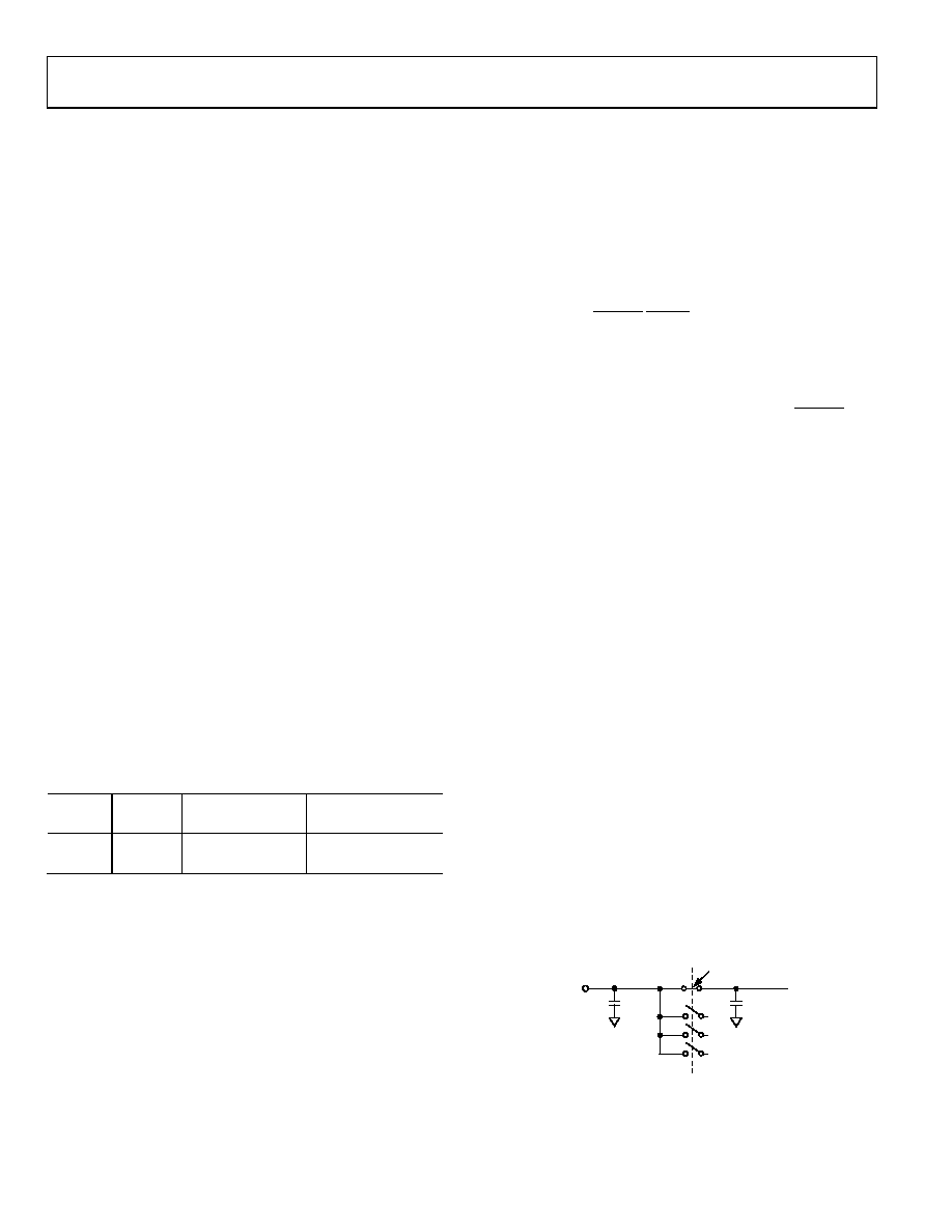
ANALOG INPUT (ISHA MODE)
Figure 19 shows the equivalent analog input circuit. The
Capacitor C1 is typically 20 pF and can be attributed to pin
capacitance and 32 off-channels. When a channel is selected, an
extra 7.5 pF (typ) is switched in. This Capacitor C2 is charged
to the previously acquired voltage on that particular channel so
it must charge/discharge to the new level. The external source
must be able to charge/discharge this additional capacitance
within 1 μs–2 μs of channel selection so that VIN can be
acquired accurately. Thus, a low impedance source is suggested.
00939-C-018
VIN
C2
7.5pF
C1
20pF
ADDRESSED CHANNEL
Figure 19. Analog Input Circuit
Large source impedances significantly affect the performance
of the ADC. An input buffer amplifier may be required.
相关PDF资料 |
PDF描述 |
|---|---|
| AD5532ABC-1 | IC DAC 14BIT 32CH 74-CSPBGA |
| AD664JNZ-UNI | IC DAC 12BIT QUAD UNIPOL 28DIP |
| AD5370BSTZ-REEL | IC DAC 16BIT 40CH SERIAL 64-LQFP |
| AD5370BCPZ-REEL7 | IC DAC 16BIT 40CH SERIAL 64LFCSP |
| VE-J5P-MW-S | CONVERTER MOD DC/DC 13.8V 100W |
相关代理商/技术参数 |
参数描述 |
|---|---|
| AD5532ABC-3 | 功能描述:IC DAC 14BIT 32CH 74-CSPBGA RoHS:否 类别:集成电路 (IC) >> 数据采集 - 数模转换器 系列:- 产品培训模块:Lead (SnPb) Finish for COTS Obsolescence Mitigation Program 标准包装:1,000 系列:- 设置时间:1µs 位数:8 数据接口:串行 转换器数目:8 电压电源:双 ± 功率耗散(最大):941mW 工作温度:0°C ~ 70°C 安装类型:表面贴装 封装/外壳:24-SOIC(0.295",7.50mm 宽) 供应商设备封装:24-SOIC W 包装:带卷 (TR) 输出数目和类型:8 电压,单极 采样率(每秒):* |
| AD5532ABC-5 | 功能描述:IC DAC 14BIT 32CH 74-CSPBGA RoHS:否 类别:集成电路 (IC) >> 数据采集 - 数模转换器 系列:- 产品培训模块:Lead (SnPb) Finish for COTS Obsolescence Mitigation Program 标准包装:1,000 系列:- 设置时间:1µs 位数:8 数据接口:串行 转换器数目:8 电压电源:双 ± 功率耗散(最大):941mW 工作温度:0°C ~ 70°C 安装类型:表面贴装 封装/外壳:24-SOIC(0.295",7.50mm 宽) 供应商设备封装:24-SOIC W 包装:带卷 (TR) 输出数目和类型:8 电压,单极 采样率(每秒):* |
| AD5532ABCZ-1 | 功能描述:IC DAC 14BIT VOUT 32CH 74-CSPBGA RoHS:是 类别:集成电路 (IC) >> 数据采集 - 数模转换器 系列:- 标准包装:1 系列:- 设置时间:4.5µs 位数:12 数据接口:串行,SPI? 转换器数目:1 电压电源:单电源 功率耗散(最大):- 工作温度:-40°C ~ 125°C 安装类型:表面贴装 封装/外壳:8-SOIC(0.154",3.90mm 宽) 供应商设备封装:8-SOICN 包装:剪切带 (CT) 输出数目和类型:1 电压,单极;1 电压,双极 采样率(每秒):* 其它名称:MCP4921T-E/SNCTMCP4921T-E/SNRCTMCP4921T-E/SNRCT-ND |
| AD5532ABCZ-1REEL | 功能描述:IC DAC 14BIT 32CH BIPO 74-CSPBGA RoHS:是 类别:集成电路 (IC) >> 数据采集 - 数模转换器 系列:- 产品培训模块:Lead (SnPb) Finish for COTS Obsolescence Mitigation Program 标准包装:1,000 系列:- 设置时间:1µs 位数:8 数据接口:串行 转换器数目:8 电压电源:双 ± 功率耗散(最大):941mW 工作温度:0°C ~ 70°C 安装类型:表面贴装 封装/外壳:24-SOIC(0.295",7.50mm 宽) 供应商设备封装:24-SOIC W 包装:带卷 (TR) 输出数目和类型:8 电压,单极 采样率(每秒):* |
| AD5532ABCZ-2 | 功能描述:IC DAC 14BIT 32CH BIPO 74-CSPBGA RoHS:是 类别:集成电路 (IC) >> 数据采集 - 数模转换器 系列:- 产品培训模块:Lead (SnPb) Finish for COTS Obsolescence Mitigation Program 标准包装:1,000 系列:- 设置时间:1µs 位数:8 数据接口:串行 转换器数目:8 电压电源:双 ± 功率耗散(最大):941mW 工作温度:0°C ~ 70°C 安装类型:表面贴装 封装/外壳:24-SOIC(0.295",7.50mm 宽) 供应商设备封装:24-SOIC W 包装:带卷 (TR) 输出数目和类型:8 电压,单极 采样率(每秒):* |
发布紧急采购,3分钟左右您将得到回复。