参数资料
| 型号: | AD5532HSABC |
| 厂商: | Analog Devices Inc |
| 文件页数: | 2/12页 |
| 文件大小: | 0K |
| 描述: | IC DAC 14BIT 32CH 74-CSPBGA |
| 产品培训模块: | Data Converter Fundamentals DAC Architectures |
| 标准包装: | 1 |
| 设置时间: | 10µs |
| 位数: | 14 |
| 数据接口: | 串行 |
| 转换器数目: | 34 |
| 电压电源: | 模拟和数字 |
| 功率耗散(最大): | 623mW |
| 工作温度: | -40°C ~ 85°C |
| 安装类型: | 表面贴装 |
| 封装/外壳: | 74-LBGA,CSPBGA |
| 供应商设备封装: | 74-CSPBGA(12x12) |
| 包装: | 托盘 |
| 输出数目和类型: | 32 电压,单极 |
| 采样率(每秒): | 1.1M |
| 配用: | EVAL-AD5532HSEBZ-ND - BOARD EVAL FOR AD5532HS EVAL-AD5532EBZ-ND - BOARD EVAL FOR AD5532 |
REV. 0
AD5532HS
–10–
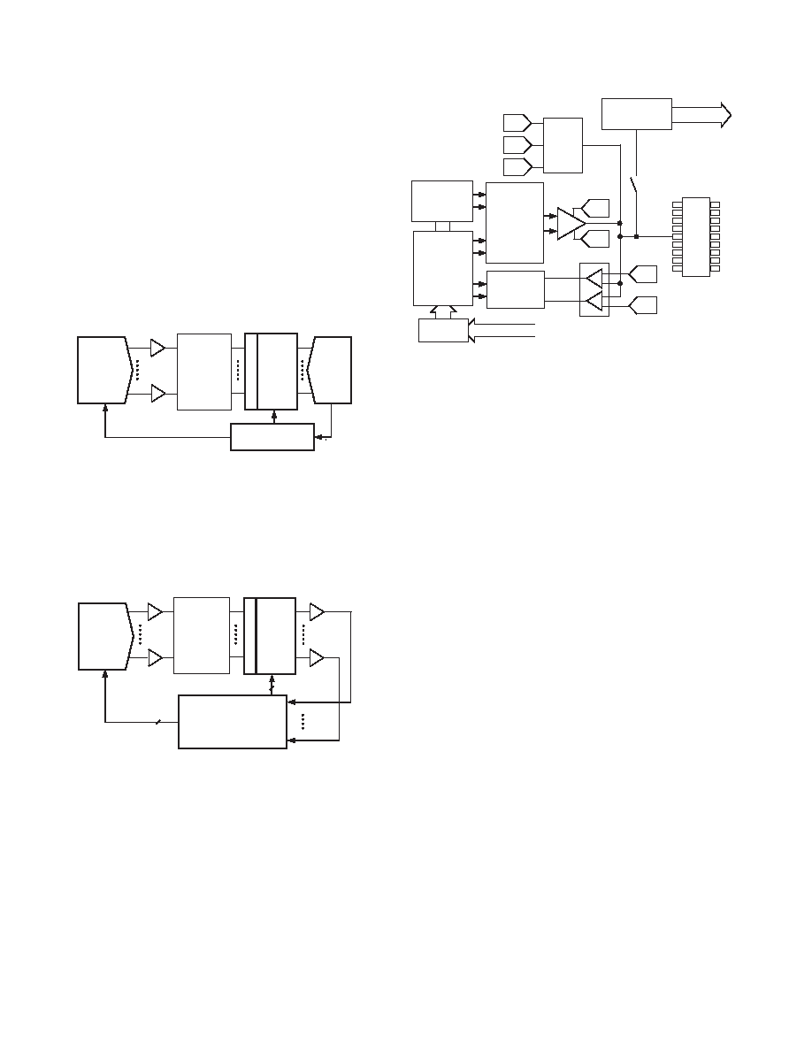
APPLICATION CIRCUITS
AD5532HS in an Optical Network Control Loop
The AD5532HS can be used in optical network applications
that require a large number of DACs to perform a control and
measurement function. In the circuit shown in Figure 7, the
0 V–5 V outputs of the AD5532HS are amplified to a range of
0 V–180 V and then used to control actuators that determine
the position of MEMS mirrors in an optical switch. The exact
position of each mirror is measured using sensors. The sensor
readings are muxed using four dual 4-channel matrix switches
(ADG739) and fed back to an 8-channel 14-bit ADC (AD7856).
The control loop is driven by an ADSP-21065L, a 32-bit SHARC
DSP with an SPI-compatible SPORT interface. It writes data
to the DAC, controls the multiplexor, and reads data from
the ADC via a 3-wire serial interface.
0V–180V
AMPS
ACTUATORS
FOR MEMS
MIRROR
ARRAY
AD7856
ADSP-21065L
S
E
N
S
O
R
S
1
32
1
32
1
8
ADG739
4
AD5532HS
Figure 7. AD5532HS and DSP Control an Optical Switch
Alternatively, the AD5532HS can be driven by an ADMC401
Motor-Controller as shown in the control-loop in Figure 8. The
DAC outputs are fed into eight AD8534 quad transconductance
amps to generate currents for voice-coil actuators that determine
the position of the mirrors. The exact position of each mirror
is measured and the readings are muxed into the on-chip
8-channel ADC of the ADMC401.
1
32
AD5532HS
AD8534
8
ADMC401
S
E
N
S
O
R
S
1
8
ADG704
8
S
P
O
R
T
3
AD8544
2
3
8-CH
12-BIT
ADC
1
8
1
32
VOICE-COIL
ACTUATORS
FOR
MEMS
MIRROR
ARRAY
Figure 8. AD5532HS and ADMC401 Control an Optical
Switch
AD5532HS in a Typical ATE System
The AD5532HS is ideally suited for use in Automatic Test
Equipment. Several DACs are required to control pin drivers,
comparators, active loads, and signal timing. Traditionally,
sample-and-hold devices were used in this application.
The AD5532HS has several advantages: no refreshing is required,
there is no droop, pedestal error is eliminated, and there is no
need for extra filtering to remove glitches. A higher level of
integration is achieved in a smaller area (see Figure 9).
DACs
ACTIVE
LOAD
DRIVER
COMPARATOR
FORMATTER
COMPARE
REGISTER
STORED
DATA
AND INHIBIT
PATTERN
PERIOD
GENERATION
AND
DELAY
TIMING
SYSTEM BUS
DUT
DAC
PARAMETRIC
MEASUREMENT
UNIT
Figure 9. AD5532HS in an ATE System
POWER SUPPLY DECOUPLING
In any circuit where accuracy is important, careful consideration
of the power supply and ground return layout helps to ensure
the rated performance. The printed circuit board on which the
AD5532HS is mounted should be designed so that the analog
and digital sections are separated, and confined to certain areas
of the board. If the AD5532HS is in a system where multiple
devices require an AGND-to-DGND connection, the connection
should be made at one point only. The star ground point should
be established as close as possible to the device. For supplies
with multiple pins (VSS, VDD, AVCC), it is recommended to
tie those pins together. The AD5532HS should have ample
supply bypassing of 10
F in parallel with 0.1 F on each supply
located as close to the package as possible, ideally right up against
the device. The 10
F capacitors are the tantalum bead type. The
0.1
F capacitor should have low Effective Series Resistance
(ESR) and Effective Series Inductance (ESI), like the common
ceramic types that provide a low impedance path to ground at
high frequencies, to handle transient currents due to internal
logic switching.
The power supply lines of the AD5532HS should use as large a
trace as possible to provide low impedance paths and reduce
the effects of glitches on the power supply line. Fast switching
signals such as clocks should be shielded with digital ground to
avoid radiating noise to other parts of the board, and should
never be run near the reference inputs. A ground line routed
between the DIN and SCLK lines will help reduce crosstalk
between them (not required on a multilayer board as there will
be a separate ground plane, but separating the lines will help). It
is essential to minimize noise on REF_IN.
Avoid crossover of digital and analog signals. Traces on opposite
sides of the board should run at right angles to each other. This
reduces the effects of feedthrough through the board. A microstrip
technique is by far the best, but not always possible with a double-
sided board. In this technique, the component side of the board
is dedicated to ground plane while signal traces are placed on
the solder side.
As is the case for all thin packages, care must be taken to avoid
flexing the package and to avoid a point load on the surface of
the package during the assembly process.
SHARC is a registered trademark of Analog Devices, Inc.
相关PDF资料 |
PDF描述 |
|---|---|
| AD5535ABCZ | IC DAC 14BIT 32CHAN 124CSPBGA |
| AD5547BRU | IC DAC 16BIT DUAL 38-TSSOP |
| AD5560JSVUZ-REEL | IC DPS PROGRAMABLE W/DAC 64TQFP |
| AD557JN | IC DAC 8BIT V-OUT 16-DIP |
| AD561KD | IC DAC 10BIT 5-15V IN MONO 16DIP |
相关代理商/技术参数 |
参数描述 |
|---|---|
| AD5532HSABCZ | 功能描述:IC DAC 14BIT 32CH HS 74-CSPBGA RoHS:是 类别:集成电路 (IC) >> 数据采集 - 数模转换器 系列:- 产品培训模块:Lead (SnPb) Finish for COTS Obsolescence Mitigation Program 标准包装:1,000 系列:- 设置时间:1µs 位数:8 数据接口:串行 转换器数目:8 电压电源:双 ± 功率耗散(最大):941mW 工作温度:0°C ~ 70°C 安装类型:表面贴装 封装/外壳:24-SOIC(0.295",7.50mm 宽) 供应商设备封装:24-SOIC W 包装:带卷 (TR) 输出数目和类型:8 电压,单极 采样率(每秒):* |
| AD5533 | 制造商:AD 制造商全称:Analog Devices 功能描述:32-Channel Infinite Sample-and-Hold |
| AD5533ABC-1 | 制造商:Analog Devices 功能描述:Sample and Hold 32-CH 16us 74-Pin CSP-BGA |
| AD5533ABC-1REEL | 制造商:Analog Devices 功能描述:Sample and Hold 32-CH 16us 74-Pin CSP-BGA T/R |
| AD5533ABCZ-1 | 制造商:Analog Devices 功能描述:Sample and Hold 32-CH 16us 74-Pin CSP-BGA |
发布紧急采购,3分钟左右您将得到回复。