参数资料
| 型号: | AD5680BRJZ-1500RL7 |
| 厂商: | Analog Devices Inc |
| 文件页数: | 5/20页 |
| 文件大小: | 0K |
| 描述: | IC DAC 18BIT 5V SOT23-8 |
| 产品培训模块: | Data Converter Fundamentals DAC Architectures |
| 标准包装: | 1 |
| 系列: | nanoDAC™ |
| 设置时间: | 80µs |
| 位数: | 18 |
| 数据接口: | DSP,MICROWIRE?,QSPI?,串行,SPI? |
| 转换器数目: | 1 |
| 电压电源: | 单电源 |
| 工作温度: | -40°C ~ 105°C |
| 安装类型: | 表面贴装 |
| 封装/外壳: | SOT-23-8 |
| 供应商设备封装: | SOT-23-8 |
| 包装: | 标准包装 |
| 输出数目和类型: | 1 电压,单极 |
| 配用: | EVAL-AD5680EBZ-ND - BOARD EVAL FOR AD5680 |
| 其它名称: | AD5680BRJZ-1500RL7DKR |
Data Sheet
AD5680
MICROPROCESSOR INTERFACING
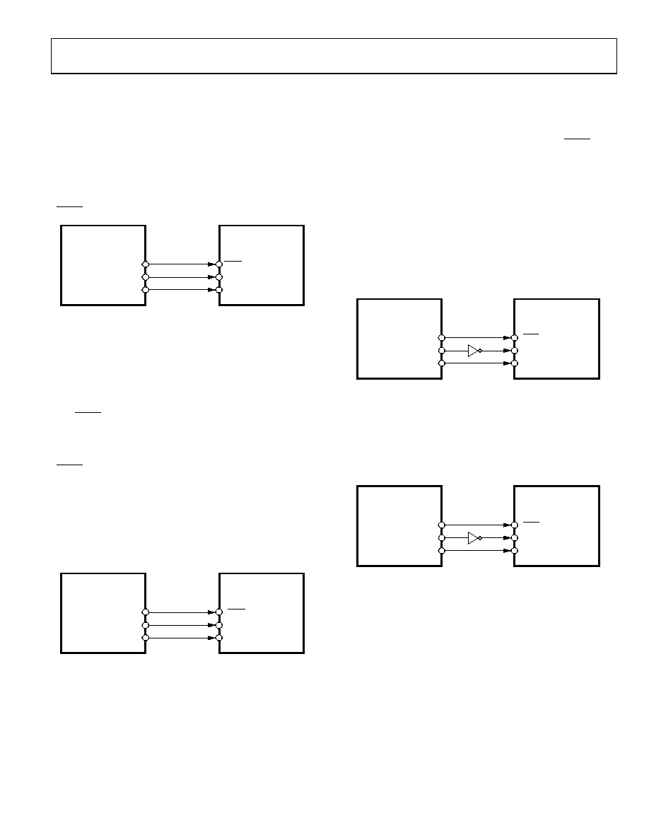
AD5680 to Blackfin ADSP-BF53x Interface
Figure 28 shows a serial interface between the AD5680 and
the Blackfin ADSP-BF53x microprocessor. The ADSP-BF53x
processor family incorporates two dual-channel synchronous
serial ports, SPORT1 and SPORT0, for serial and multiprocessor
communications. Using SPORT0 to connect to the AD5680, the
setup for the interface is as follows. DT0PRI drives the DIN pin
of the AD5680, while TSCLK0 drives the SCLK of the part. The
SYNC is driven from TFS0.
AD5680*
*ADDITIONAL PINS OMITTED FOR CLARITY.
TFS0
DTOPRI
TSCLK0
SYNC
DIN
SCLK
05854-
035
ADSP-BF53x*
Figure 28. AD5680 to Blackfin ADSP-BF53x Interface
AD5680 to 68HC11/68L11 Interface
Figure 29 shows a serial interface between the AD5680 and the
68HC11/68L11 microcontroller. SCK of the 68HC11/68L11
drives the SCLK of the AD5680, while the MOSI output drives
the serial data line of the DAC.
The SYNC signal is derived from a port line (PC7). The setup
conditions for correct operation of this interface are as follows:
The 68HC11/68L11 is configured with its CPOL bit as 0 and its
CPHA bit as 1. When data is being transmitted to the DAC, the
SYNC line is taken low (PC7). When the 68HC11/68L11 is
configured this way, data appearing on the MOSI output is valid
on the falling edge of SCK. Serial data from the 68HC11/68L11
is transmitted in 8-bit bytes with only eight falling clock edges
occurring in the transmit cycle. Data is transmitted MSB first. To
load data to the AD5680, PC7 is left low after the first eight bits
are transferred, and a second serial write operation is performed
to the DAC; PC7 is taken high at the end of this procedure.
AD5680*
*ADDITIONAL PINS OMITTED FOR CLARITY.
PC7
SCK
MOSI
SYNC
SCLK
DIN
05854-
036
68HC11/68L11*
Figure 29. AD5680 to 68HC11/68L11 Interface
AD5680 to 80C51/80L51 Interface
80C51/80L51 microcontroller. The setup for the interface is as
follows. TxD of the 80C51/80L51 drives SCLK of the AD5680,
while RxD drives the serial data line of the part. The SYNC
signal is again derived from a bit-programmable pin on the port.
In this case, port line P3.3 is used. When data is to be transmitted
to the AD5680, P3.3 is taken low. The 80C51/80L51 transmits
data in 8-bit bytes only; thus, only eight falling clock edges occur
in the transmit cycle. To load data to the DAC, P3.3 is left low
after the first eight bits are transmitted, and a second write cycle
is initiated to transmit the second byte of data. P3.3 is taken
high following the completion of this cycle. The 80C51/80L51
outputs the serial data in a format that has the LSB first. The
AD5680 must receive data with the MSB first. The 80C51/80L51
transmit routine should take this into account.
80C51/80L51*
AD5680*
*ADDITIONAL PINS OMITTED FOR CLARITY.
P3.3
TxD
RxD
SYNC
SCLK
DIN
05854-
037
Figure 30. AD5680 to 80C51/80L51 Interface
AD5680 to MICROWIRE Interface
MICROWIRE-compatible device. Serial data is shifted out on
the falling edge of the serial clock and is clocked into the AD5680
on the rising edge of the SK.
MICROWIRE*
AD5680*
*ADDITIONAL PINS OMITTED FOR CLARITY.
CS
SK
SO
SYNC
SCLK
DIN
05854-
038
Figure 31. AD5680 to MICROWIRE Interface
Rev. B | Page 13 of 20
相关PDF资料 |
PDF描述 |
|---|---|
| LTC1257CN8#PBF | IC D/A CONV 12BIT VOLT OUT 8-DIP |
| MS27468E25A2PB | CONN RCPT 100POS JAM NUT W/PINS |
| ICS87972DYI-147LFT | IC CLK MULT/ZD BUFFER 52-LQFP |
| AD5664BCPZ-REEL7 | IC DAC NANO 16BIT QUAD 10-LFCSP |
| D38999/26MC4SE | CONN PLUG 4POS STRAIGHT W/SCKT |
相关代理商/技术参数 |
参数描述 |
|---|---|
| AD5680BRJZ-1REEL7 | 制造商:AD 制造商全称:Analog Devices 功能描述:5 V 18-Bit nanoDAC in a SOT-23 |
| AD5680BRJZ-2500RL7 | 功能描述:IC DAC 18BIT 5V SOT23-8 RoHS:是 类别:集成电路 (IC) >> 数据采集 - 数模转换器 系列:nanoDAC™ 产品培训模块:Lead (SnPb) Finish for COTS Obsolescence Mitigation Program 标准包装:50 系列:- 设置时间:4µs 位数:12 数据接口:串行 转换器数目:2 电压电源:单电源 功率耗散(最大):- 工作温度:-40°C ~ 85°C 安装类型:表面贴装 封装/外壳:8-TSSOP,8-MSOP(0.118",3.00mm 宽) 供应商设备封装:8-uMAX 包装:管件 输出数目和类型:2 电压,单极 采样率(每秒):* 产品目录页面:1398 (CN2011-ZH PDF) |
| AD5680BRJZ-2REEL7 | 功能描述:IC DAC 18BIT 5V SOT23-8 RoHS:是 类别:集成电路 (IC) >> 数据采集 - 数模转换器 系列:nanoDAC™ 产品培训模块:Lead (SnPb) Finish for COTS Obsolescence Mitigation Program 标准包装:50 系列:- 设置时间:4µs 位数:12 数据接口:串行 转换器数目:2 电压电源:单电源 功率耗散(最大):- 工作温度:-40°C ~ 85°C 安装类型:表面贴装 封装/外壳:8-TSSOP,8-MSOP(0.118",3.00mm 宽) 供应商设备封装:8-uMAX 包装:管件 输出数目和类型:2 电压,单极 采样率(每秒):* 产品目录页面:1398 (CN2011-ZH PDF) |
| AD5681RBCPZ-1RL | 功能描述:12 Bit Digital to Analog Converter 1 8-LFCSP-UD (2x2) 制造商:analog devices inc. 系列:nanoDAC+? 包装:带卷(TR) 零件状态:过期 位数:12 数模转换器数:1 建立时间:7μs 输出类型:Voltage - Buffered 差分输出:无 数据接口:SPI 参考类型:外部, 内部 电压 - 电源,模拟:2.7 V ~ 5.5 V 电压 - 电源,数字:1.8 V ~ 5.5 V INL/DNL(LSB):±1(最大),±1(最大) 架构:电阻串 DAC 工作温度:-40°C ~ 105°C 封装/外壳:8-UFDFN 裸露焊盘,CSP 供应商器件封装:8-LFCSP-UD(2x2) 标准包装:10,000 |
| AD5681RBCPZ-1RL7 | 功能描述:IC DAC 12BIT SPI 8LFCSP 制造商:analog devices inc. 系列:nanoDAC+? 包装:剪切带(CT) 零件状态:在售 位数:12 数模转换器数:1 建立时间:7μs 输出类型:Voltage - Buffered 差分输出:无 数据接口:SPI 参考类型:外部, 内部 电压 - 电源,模拟:2.7 V ~ 5.5 V 电压 - 电源,数字:1.8 V ~ 5.5 V INL/DNL(LSB):±1(最大),±1(最大) 架构:电阻串 DAC 工作温度:-40°C ~ 105°C 封装/外壳:8-UFDFN 裸露焊盘,CSP 供应商器件封装:8-LFCSP-UD(2x2) 标准包装:1 |
发布紧急采购,3分钟左右您将得到回复。