- 您现在的位置:买卖IC网 > PDF目录223307 > AD573* 10-Bit A/D Converter PDF资料下载
参数资料
| 型号: | AD573* |
| 英文描述: | 10-Bit A/D Converter |
| 中文描述: | 10位A / D转换器 |
| 文件页数: | 5/8页 |
| 文件大小: | 327K |
AD573
REV. A
–5–
BIPOLAR CONNECTION
To obtain the bipolar –5 V to +5 V range with an offset binary
output code, the bipolar offset control pin is left open.
A –5.000 volt signal will give a 10-bit code of 00000000 00; an
input of 0.000 volts results in an output code of 10000000 00
and +4.99 volts at the input yields the 11111111 11 code. The
nominal transfer curve is shown in Figure 6.
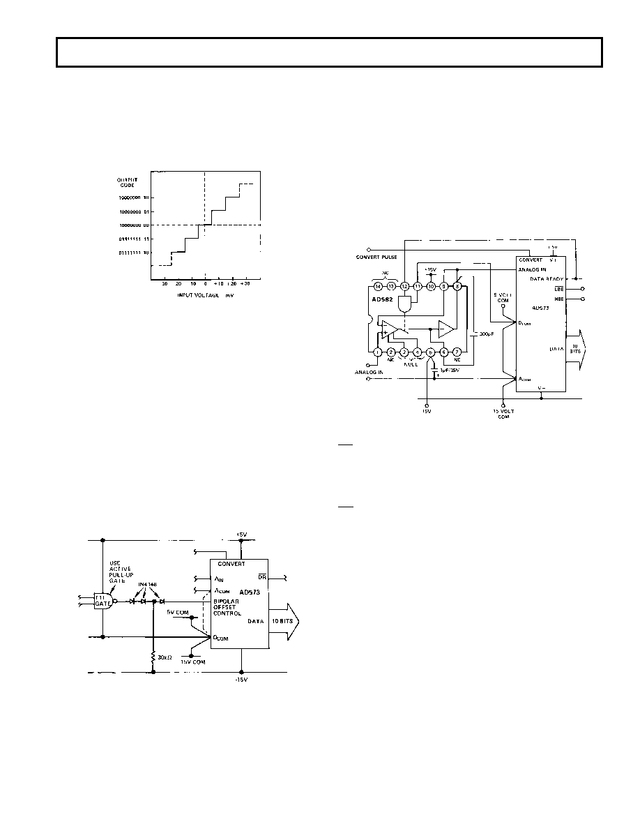
Figure 6. AD573 Transfer Curve— Bipolar Operation
Note that in the bipolar mode, the code transitions are offset
1/2 LSB such that an input voltage of 0 volts
±5 mV yields the
code representing zero (10000000 00). Each output code is then
centered on its nominal input voltage.
Full-Scale Calibration
Full-Scale Calibration is accomplished in the same manner as in
unipolar operation except the full scale input voltage is +4.985
volts.
Negative Full-Scale Calibration
The circuit in Figure 4a can also be used in bipolar operation to
offset the input voltage (nominally –5 V) which results in the
00000000 00 code. R2 should be omitted to obtain a symmetri-
cal range.
The bipolar offset control input is not directly TTL compatible
but a TTL interface for logic control can be constructed as
shown in Figure 7.
Figure 7. Bipolar Offset Controlled by Logic Gate
Gate Output = 1 Unipolar 0–10 V Input Range
Gate Output = 0 Bipolar
±5 V Input Range
SAMPLE-HOLD AMPLIFIER CONNECTION TO THE
AD573
Many situations in high speed acquisition systems or digitizing
rapidly changing signals require a sample-hold amplifier (SHA)
in front of the A/D converter. The SHA can acquire and hold a
signal faster than the converter can perform a conversion. A
SHA can also be used to accurately define the exact point in
time at which the signal is sampled. For the AD573, a SHA can
also serve as a high input impedance buffer.
Figure 8 shows the AD573 connected to the AD582 monolithic
SHA for high speed signal acquisition. In this configuration, the
AD582 will acquire a 10 volt signal in less than 10
s with a
droop rate less than 100
V/ms.
Figure 8. Sample-Hold Interface to the AD573
DR
goes high after the conversion is initiated to indicate that
reset of the SAR is complete. In Figure 8 it is also used to put
the AD582 into the hold mode while the AD573 begins its con-
version cycle. (The AD582 settles to final value well in advance
of the first comparator decision inside the AD573).
DR
goes low when the conversion is complete placing the
AD582 back in the sample mode. Configured as shown in Fig-
ure 8, the next conversion can be initiated after a 10
s delay to
allow for signal acquisition by the AD582.
Observe carefully the ground, supply, and bypass capacitor con-
nections between the two devices. This will minimize ground
noise and interference during the conversion cycle.
GROUNDING CONSIDERATIONS
The AD573 provides separate Analog and Digital Common
connections. The circuit will operate properly with as much as
±200 mV of common-mode voltage between the two commons.
This permits more flexible control of system common bussing
and digital and analog returns.
In normal operation, the Analog Common terminal may gener-
ate transient currents of up to 2 mA during a conversion. In ad-
dition a static current of about 2 mA will flow into Analog
Common in the unipolar mode after a conversion is complete.
The Analog Common current will be modulated by the varia-
tions in input signal.
The absolute maximum voltage rating between the two com-
mons is
±1 volt. It is recommended that a parallel pair of
back-to-back protection diodes be connected between the com-
mons if they are not connected locally.
相关PDF资料 |
PDF描述 |
|---|---|
| AD574ATD | Analog-to-Digital Converter??? 12-Bit |
| AD574AUD | Analog-to-Digital Converter??? 12-Bit |
| AD575JD | Analog-to-Digital Converter, 10-Bit |
| AD575JN | Analog-to-Digital Converter, 10-Bit |
| AD575KD | Analog-to-Digital Converter, 10-Bit |
相关代理商/技术参数 |
参数描述 |
|---|---|
| AD5732 | 制造商:AD 制造商全称:Analog Devices 功能描述:Complete, Dual, 12-/14-/16-Bit, Serial Input, Unipolar/Bipolar, Voltage Output DACs |
| AD5732AREZ | 功能描述:IC DAC DUAL 14BIT SERIAL 24TSSOP RoHS:是 类别:集成电路 (IC) >> 数据采集 - 数模转换器 系列:- 标准包装:1 系列:- 设置时间:4.5µs 位数:12 数据接口:串行,SPI? 转换器数目:1 电压电源:单电源 功率耗散(最大):- 工作温度:-40°C ~ 125°C 安装类型:表面贴装 封装/外壳:8-SOIC(0.154",3.90mm 宽) 供应商设备封装:8-SOICN 包装:剪切带 (CT) 输出数目和类型:1 电压,单极;1 电压,双极 采样率(每秒):* 其它名称:MCP4921T-E/SNCTMCP4921T-E/SNRCTMCP4921T-E/SNRCT-ND |
| AD5732AREZ-REEL7 | 功能描述:IC DAC DUAL 14BIT SERIAL 24TSSOP RoHS:是 类别:集成电路 (IC) >> 数据采集 - 数模转换器 系列:- 标准包装:47 系列:- 设置时间:2µs 位数:14 数据接口:并联 转换器数目:1 电压电源:单电源 功率耗散(最大):55µW 工作温度:-40°C ~ 85°C 安装类型:表面贴装 封装/外壳:28-SSOP(0.209",5.30mm 宽) 供应商设备封装:28-SSOP 包装:管件 输出数目和类型:1 电流,单极;1 电流,双极 采样率(每秒):* |
| AD5732R | 制造商:AD 制造商全称:Analog Devices 功能描述:Complete, Dual, 12-/14-/16-Bit, Serial Input, Unipolar/Bipolar, Voltage Output DACs |
发布紧急采购,3分钟左右您将得到回复。