- 您现在的位置:买卖IC网 > PDF目录223307 > AD573* 10-Bit A/D Converter PDF资料下载
参数资料
| 型号: | AD573* |
| 英文描述: | 10-Bit A/D Converter |
| 中文描述: | 10位A / D转换器 |
| 文件页数: | 8/8页 |
| 文件大小: | 327K |
AD573
REV. A
–8–
C841–9–5/84
PRINTED
IN
U.S.A.
It is also possible to write a faster-executing assembly-language
routine to control the AD573. Such a routine will require a de-
lay between starting and reading the converter. This can be eas-
ily implemented by calling the Apple’s WAIT subroutine (which
resides at location $FCA8) after loading the accumulator with a
number greater than or equal to two.
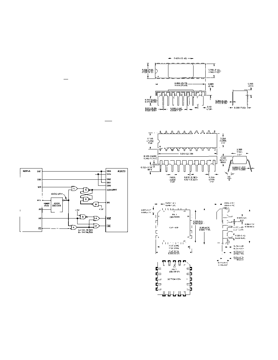
8085-Series Microprocessor Interface
The AD573 can also be used with 8085-series microprocessors.
These processors use separate control signals for RD and WR,
as opposed to the single R/W control signal used in the 6800/
6500 series processors.
There are two constraints related to operation of the AD573
with 8085-series processors. The first problem is the width of
the CONVERT pulse. The circuit shown in Figure 17 (essen-
tially the same as that shown in Figure 13) will produce a wide
enough CONVERT pulse when the 8085 is running at 5 MHz.
For 8085 systems running at slower clock rates (3 MHz), the
flip-flop-based circuit can be eliminated since the WR pulse will
be approximately 500 ns wide.
The other consideration is the access time of the AD573’s three-
state output data buffers, which is 250 ns maximum. It may be
necessary to insert wait states during RD operations from the
AD573. This will not be a problem in systems using memories
with comparable access times, since wait states will have already
been provided in the basic system design.
Figure 17. AD573–8085A Interface Connections
The following assembly-language subroutine can be used to
control an AD573 residing at memory locations 3000H and
3001H. The 10 bits of data are returned (left-justified) in the
DE register pair.
ADC:
LXI H, 3000 ; LOAD HL WITH AD573 ADDRESS
MOV M, A
; START CONVERSION
MVI B, 06
; LOAD DELAY PERIOD
LOOP: DCR B
; DELAY LOOP
JNZ LOOP
;
MOV A, M
; READ LOW BYTE
ANI C0
; MASK LOWER 6 BITS
MOV E, A
; STORE CLEAN LOW BYTE IN E
INR L
; LOAD HIGH BYTE ADDRESS
MOV D, M
; MOVE HIGH BYTE TO D
RET
; EXIT
OUTLINE DIMENSIONS
Dimensions shown in inches and (mm).
20-Pin Ceramic DIP Package (“D”)
20-Pin Plastic DIP Package (“N”)
P-20A PLCC
相关PDF资料 |
PDF描述 |
|---|---|
| AD574ATD | Analog-to-Digital Converter??? 12-Bit |
| AD574AUD | Analog-to-Digital Converter??? 12-Bit |
| AD575JD | Analog-to-Digital Converter, 10-Bit |
| AD575JN | Analog-to-Digital Converter, 10-Bit |
| AD575KD | Analog-to-Digital Converter, 10-Bit |
相关代理商/技术参数 |
参数描述 |
|---|---|
| AD5732 | 制造商:AD 制造商全称:Analog Devices 功能描述:Complete, Dual, 12-/14-/16-Bit, Serial Input, Unipolar/Bipolar, Voltage Output DACs |
| AD5732AREZ | 功能描述:IC DAC DUAL 14BIT SERIAL 24TSSOP RoHS:是 类别:集成电路 (IC) >> 数据采集 - 数模转换器 系列:- 标准包装:1 系列:- 设置时间:4.5µs 位数:12 数据接口:串行,SPI? 转换器数目:1 电压电源:单电源 功率耗散(最大):- 工作温度:-40°C ~ 125°C 安装类型:表面贴装 封装/外壳:8-SOIC(0.154",3.90mm 宽) 供应商设备封装:8-SOICN 包装:剪切带 (CT) 输出数目和类型:1 电压,单极;1 电压,双极 采样率(每秒):* 其它名称:MCP4921T-E/SNCTMCP4921T-E/SNRCTMCP4921T-E/SNRCT-ND |
| AD5732AREZ-REEL7 | 功能描述:IC DAC DUAL 14BIT SERIAL 24TSSOP RoHS:是 类别:集成电路 (IC) >> 数据采集 - 数模转换器 系列:- 标准包装:47 系列:- 设置时间:2µs 位数:14 数据接口:并联 转换器数目:1 电压电源:单电源 功率耗散(最大):55µW 工作温度:-40°C ~ 85°C 安装类型:表面贴装 封装/外壳:28-SSOP(0.209",5.30mm 宽) 供应商设备封装:28-SSOP 包装:管件 输出数目和类型:1 电流,单极;1 电流,双极 采样率(每秒):* |
| AD5732R | 制造商:AD 制造商全称:Analog Devices 功能描述:Complete, Dual, 12-/14-/16-Bit, Serial Input, Unipolar/Bipolar, Voltage Output DACs |
发布紧急采购,3分钟左右您将得到回复。