- 您现在的位置:买卖IC网 > PDF目录10066 > AD573JN (Analog Devices Inc)IC ADC 10BIT SAR REGISTER 20-DIP PDF资料下载
参数资料
| 型号: | AD573JN |
| 厂商: | Analog Devices Inc |
| 文件页数: | 4/10页 |
| 文件大小: | 0K |
| 描述: | IC ADC 10BIT SAR REGISTER 20-DIP |
| 标准包装: | 1 |
| 位数: | 10 |
| 采样率(每秒): | 50k |
| 数据接口: | 并联 |
| 转换器数目: | 1 |
| 功率耗散(最大): | 800mW |
| 电压电源: | 双 ± |
| 工作温度: | 0°C ~ 70°C |
| 安装类型: | 通孔 |
| 封装/外壳: | 20-DIP(0.300",7.62mm) |
| 供应商设备封装: | 20-PDIP |
| 包装: | 管件 |
| 输入数目和类型: | 1 个单端,单极;1 个单端,双极 |
AD573
–3–
ABSOLUTE MAXIMUM RATINGS
V+ to Digital Common . . . . . . . . . . . . . . . . . . . . . 0 V to +7 V
V– to Digital Common . . . . . . . . . . . . . . . . . . . 0 V to –16.5 V
Analog Common to Digital Common . . . . . . . . . . . . . . .
±1 V
Analog Input to Analog Common . . . . . . . . . . . . . . . . .
±15 V
Control Inputs . . . . . . . . . . . . . . . . . . . . . . . . . . . . . . 0 V to V+
Digital Outputs (High Impedance State) . . . . . . . . . . 0 V to V+
Power Dissipation . . . . . . . . . . . . . . . . . . . . . . . . . . . . 800 mW
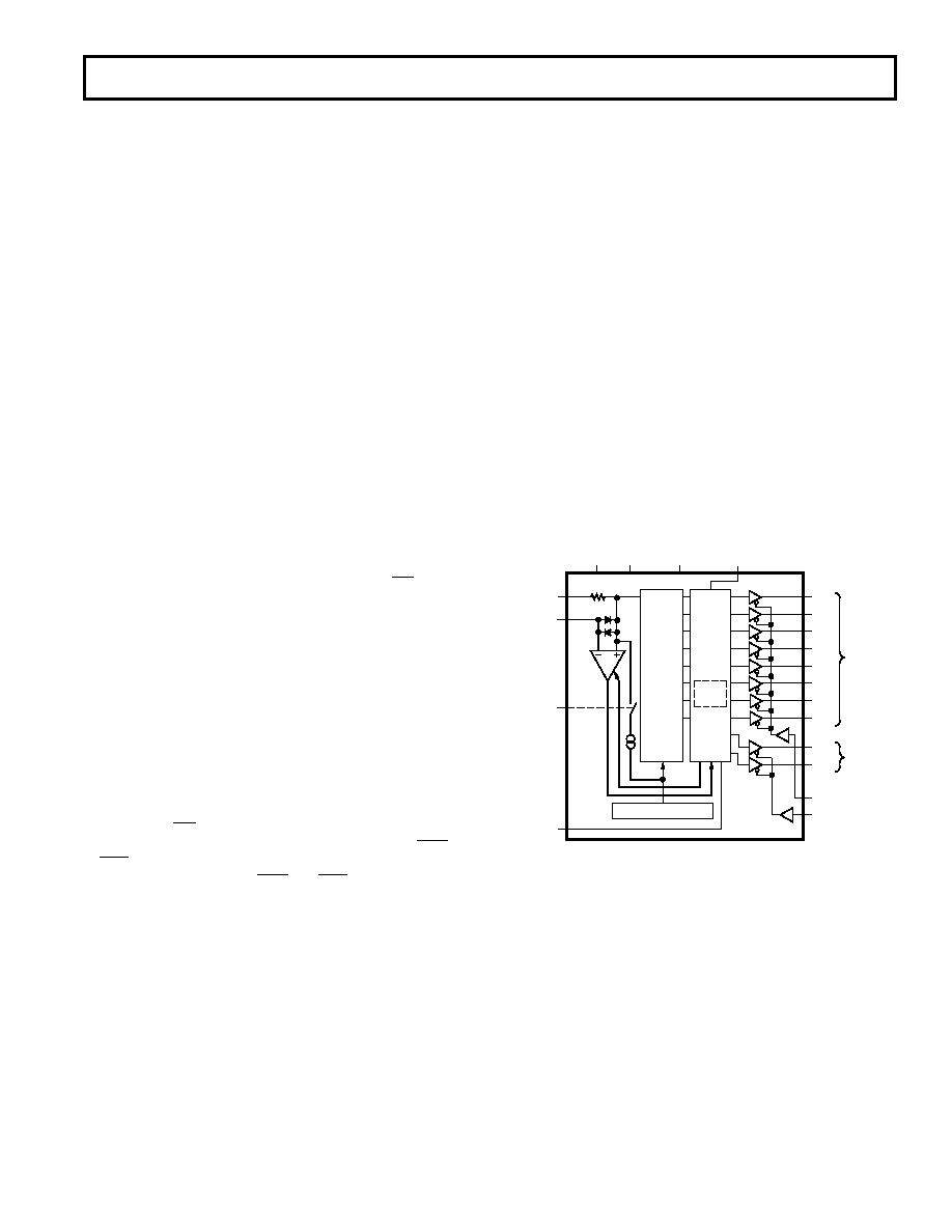
FUNCTIONAL DESCRIPTION
A block diagram of the AD573 is shown in Figure 1. The posi-
tive CONVERT pulse must be at least 500 ns wide. DR goes
high within 1.5
s after the leading edge of the convert pulse
indicating that the internal logic has been reset. The negative
edge of the CONVERT pulse initiates the conversion. The in-
ternal 10-bit current output DAC is sequenced by the integrated
injection logic (I
2L) successive approximation register (SAR)
from its most significant bit to least significant bit to provide an
output current which accurately balances the input signal cur-
rent through the 5 k
resistor. The comparator determines
whether the addition of each successively weighted bit current
causes the DAC current sum to be greater or less than the input
current; if the sum is more, the bit is turned off. After testing all
bits, the SAR contains a 10-bit binary code which accurately
represents the input signal to within 1/2 LSB (0.05% of full scale).
The SAR drives DR low to indicate that the conversion is com-
plete and that the data is available to the output buffers. HBE
and LBE can then be activated to enable the upper 8-bit and
lower 2-bit buffers as desired. HBE and LBE should be brought
high prior to the next conversion to place the output buffers in
the high impedance state.
The temperature compensated buried Zener reference provides
the primary voltage reference to the DAC and ensures excellent
stability with both time and temperature. The bipolar offset in-
put controls a switch which allows the positive bipolar offset
current (exactly equal to the value of the MSB less 1/2 LSB) to
be injected into the summing (+) node of the comparator to
offset the DAC output. Thus the nominal 0 V to +10 V unipolar
input range becomes a –5 V to +5 V range. The 5 k
thin-film
input resistor is trimmed so that with a full-scale input signal, an
input current will be generated which exactly matches the DAC
output with all bits on.
BURIED ZENER REF
COMP-
ARATOR
ANALOG
IN
DB9
HIGH
BYTE
10-BIT
CURRENT
OUTPUT
DAC
V+
V–
DIGITAL
COMMON
CONVERT
INT
CLOCK
10-BIT
SAR
DB8
DB7
DB6
DB5
DB4
DB3
DB2
DB1
DB0
HBE
LBE
MSB
LSB
LOW
BYTE
ANALOG
COMMON
BIPOLAR
OFFSET
CONTROL
DATA
READY
AD573
5k
Figure 1. Functional Block Diagram
UNIPOLAR CONNECTION
The AD573 contains all the active components required to per-
form a complete A/D conversion. Thus, for many applications,
all that is necessary is connection of the power supplies (+5 V
and –12 V to –15 V), the analog input and the convert pulse.
However, there are some features and special connections which
should be considered for achieving optimum performance. The
functional pinout is shown in Figure 2.
The standard unipolar 0 V to +10 V range is obtained by short-
ing the bipolar offset control pin (Pin 16) to digital common
(Pin 17).
REV. B
相关PDF资料 |
PDF描述 |
|---|---|
| LT1342CG#TR | IC TXRX 5V RS232 3V LOGIC 28SSOP |
| LTC1384IN#PBF | IC TXRX 5V RS232 LOW PWR 18-DIP |
| LTC1384IN | IC TXRX 5V RS232 LOW PWR 18-DIP |
| IDT72231L10PF | IC FIFO SYNC 512X9 10NS 32QFP |
| MS3106A22-12P | CONN PLUG 5POS STRAIGHT W/PINS |
相关代理商/技术参数 |
参数描述 |
|---|---|
| AD573JNZ | 功能描述:IC ADC 10BIT SAR REGISTER 20-DIP RoHS:是 类别:集成电路 (IC) >> 数据采集 - 模数转换器 系列:- 标准包装:1 系列:microPOWER™ 位数:8 采样率(每秒):1M 数据接口:串行,SPI? 转换器数目:1 功率耗散(最大):- 电压电源:模拟和数字 工作温度:-40°C ~ 125°C 安装类型:表面贴装 封装/外壳:24-VFQFN 裸露焊盘 供应商设备封装:24-VQFN 裸露焊盘(4x4) 包装:Digi-Reel® 输入数目和类型:8 个单端,单极 产品目录页面:892 (CN2011-ZH PDF) 其它名称:296-25851-6 |
| AD573JP | 功能描述:IC ADC 10BIT SAR REGISTER 20PLCC RoHS:否 类别:集成电路 (IC) >> 数据采集 - 模数转换器 系列:- 标准包装:1 系列:- 位数:14 采样率(每秒):83k 数据接口:串行,并联 转换器数目:1 功率耗散(最大):95mW 电压电源:双 ± 工作温度:0°C ~ 70°C 安装类型:通孔 封装/外壳:28-DIP(0.600",15.24mm) 供应商设备封装:28-PDIP 包装:管件 输入数目和类型:1 个单端,双极 |
| AD573JPZ | 功能描述:IC ADC 10BIT SAR REGISTER 20PLCC RoHS:是 类别:集成电路 (IC) >> 数据采集 - 模数转换器 系列:- 标准包装:1 系列:- 位数:14 采样率(每秒):83k 数据接口:串行,并联 转换器数目:1 功率耗散(最大):95mW 电压电源:双 ± 工作温度:0°C ~ 70°C 安装类型:通孔 封装/外壳:28-DIP(0.600",15.24mm) 供应商设备封装:28-PDIP 包装:管件 输入数目和类型:1 个单端,双极 |
| AD573KD | 功能描述:IC ADC 10BIT SAR REG 20-CDIP RoHS:否 类别:集成电路 (IC) >> 数据采集 - 模数转换器 系列:- 产品培训模块:Lead (SnPb) Finish for COTS Obsolescence Mitigation Program 标准包装:250 系列:- 位数:12 采样率(每秒):1.8M 数据接口:并联 转换器数目:1 功率耗散(最大):1.82W 电压电源:模拟和数字 工作温度:-40°C ~ 85°C 安装类型:表面贴装 封装/外壳:48-LQFP 供应商设备封装:48-LQFP(7x7) 包装:管件 输入数目和类型:2 个单端,单极 |
| AD573KD/+ | 制造商:Rochester Electronics LLC 功能描述:- Bulk |
发布紧急采购,3分钟左右您将得到回复。