- 您现在的位置:买卖IC网 > PDF目录10066 > AD573JN (Analog Devices Inc)IC ADC 10BIT SAR REGISTER 20-DIP PDF资料下载
参数资料
| 型号: | AD573JN |
| 厂商: | Analog Devices Inc |
| 文件页数: | 7/10页 |
| 文件大小: | 0K |
| 描述: | IC ADC 10BIT SAR REGISTER 20-DIP |
| 标准包装: | 1 |
| 位数: | 10 |
| 采样率(每秒): | 50k |
| 数据接口: | 并联 |
| 转换器数目: | 1 |
| 功率耗散(最大): | 800mW |
| 电压电源: | 双 ± |
| 工作温度: | 0°C ~ 70°C |
| 安装类型: | 通孔 |
| 封装/外壳: | 20-DIP(0.300",7.62mm) |
| 供应商设备封装: | 20-PDIP |
| 包装: | 管件 |
| 输入数目和类型: | 1 个单端,单极;1 个单端,双极 |
AD573
–6–
CONTROL AND TIMING OF THE AD573
The operation of the AD573 is controlled by three inputs:
CONVERT
, HBE and LBE.
Starting a Conversion
The conversion cycle is initiated by a positive going CONVERT
pulse at least 500 ns wide. The rising edge of this pulse resets
the internal logic, clears the result of the previous conversion,
and sets DR high. The falling edge of CONVERT begins the
conversion cycle. When conversion is completed DR returns
low. During the conversion cycle, HBE and LBE should be held
high. If HBE or LBE goes low during a conversion, the data
output buffers will be enabled and intermediate conversion re-
sults will be present on the data output pins. This may cause
bus conflicts if other devices in a system are trying to use the bus.
tCS
tDSC
VOH + VOL
2
VIH + VIL
2
tC
CONVERT
DR
Figure 9. Convert Timing
Reading the Data
The three-state data output buffers are enabled by HBE and
LBE
. Access time of these buffers is typically 150 ns (250 maxi-
mum). The data outputs remain valid until 50 ns after the en-
able signal returns high, and are completely into the high
impedance state 100 ns later.
VIH + VIL
2
LBE OR HBE
tHD
tDD
VOH
VOL
DATA
VALID
tHL
HIGH
IMPEDANCE
HIGH
IMPEDANCE
DB0–DB7
OR
DB8–DB9
Figure 10. Read Timing
TIMING SPECIFICATIONS (All grades, TA = TMIN–TMAX)
Parameter
Symbol Min Typ
Max Units
CONVERT Pulse Width
tCS
500 –
–
ns
DR
Delay from CONVERT tDSC
–
1
1.5
s
Conversion Time
tC
10
20
30
s
Data Access Time
tDD
0
150
250
ns
Data Valid after HBE/LBE
High
tHD
50
–
ns
Output Float Delay
tHL
–
100
200
ns
MICROPROCESSOR INTERFACE CONSIDERATIONS—
GENERAL
When an analog-to-digital converter like the AD573 is inter-
faced to a microprocessor, several details of the interface must
be considered. First, a signal to start the converter must be gen-
erated; then an appropriate delay period must be allowed to pass
before valid conversion data may be read. In most applications,
the AD573 can interface to a microprocessor system with little
or no external logic.
The most popular control signal configuration consists of de-
coding the address assigned to the AD573, then gating this sig-
nal with the system’s WR signal to generate the CONVERT
pulse, and gating it with RD to enable the output buffers. The
use of a memory address and memory WR and RD signals de-
notes “memory-mapped” I/O interfacing, while the use of a
separate I/O address space denotes “isolated I/O” interfacing. In
8-bit bus systems, the 10-bit AD573 will occupy two locations
when data is to be read; therefore, two (usually consecutive) ad-
dresses must be decoded. One of the addresses can also be used
as the address which produces the CONVERT signal during
WR operations.
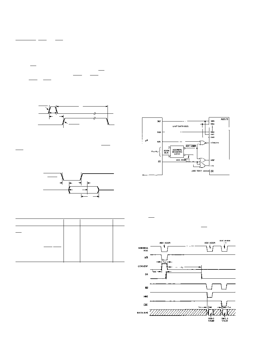
Figure 11 shows a generalized diagram of the control logic for
an AD573 interfaced to an 8-bit data bus, where two addresses
(ADC ADDR and ADC ADDR + 1) have been decoded. ADC
ADDR starts the converter when written to (the actual data be-
ing written to the converter does not matter) and contains the
high byte data during read operations. ADC ADDR + 1 per-
forms no function during write operations, but contains the low
byte data during read operations.
Figure 11. General AD573 Interface to 8-Bit Microprocessor
In systems where this read-write interface is used, at least 30
microseconds (the maximum conversion time) must be allowed
to pass between starting a conversion and reading the results.
This delay or “timeout” period can be implemented in a short
software routine such as a countdown loop, enough dummy in-
structions to consume 30 microseconds, or enough actual useful
instructions to consume the required time. In tightly-timed sys-
tems, the DR line may be read through an external three-state
buffer to determine precisely when a conversion is complete.
Higher speed systems may choose to use DR to signal an inter-
rupt to the processor at the end of a conversion.
Figure 12. Typical AD573 Interface Timing Diagram
REV. B
相关PDF资料 |
PDF描述 |
|---|---|
| LT1342CG#TR | IC TXRX 5V RS232 3V LOGIC 28SSOP |
| LTC1384IN#PBF | IC TXRX 5V RS232 LOW PWR 18-DIP |
| LTC1384IN | IC TXRX 5V RS232 LOW PWR 18-DIP |
| IDT72231L10PF | IC FIFO SYNC 512X9 10NS 32QFP |
| MS3106A22-12P | CONN PLUG 5POS STRAIGHT W/PINS |
相关代理商/技术参数 |
参数描述 |
|---|---|
| AD573JNZ | 功能描述:IC ADC 10BIT SAR REGISTER 20-DIP RoHS:是 类别:集成电路 (IC) >> 数据采集 - 模数转换器 系列:- 标准包装:1 系列:microPOWER™ 位数:8 采样率(每秒):1M 数据接口:串行,SPI? 转换器数目:1 功率耗散(最大):- 电压电源:模拟和数字 工作温度:-40°C ~ 125°C 安装类型:表面贴装 封装/外壳:24-VFQFN 裸露焊盘 供应商设备封装:24-VQFN 裸露焊盘(4x4) 包装:Digi-Reel® 输入数目和类型:8 个单端,单极 产品目录页面:892 (CN2011-ZH PDF) 其它名称:296-25851-6 |
| AD573JP | 功能描述:IC ADC 10BIT SAR REGISTER 20PLCC RoHS:否 类别:集成电路 (IC) >> 数据采集 - 模数转换器 系列:- 标准包装:1 系列:- 位数:14 采样率(每秒):83k 数据接口:串行,并联 转换器数目:1 功率耗散(最大):95mW 电压电源:双 ± 工作温度:0°C ~ 70°C 安装类型:通孔 封装/外壳:28-DIP(0.600",15.24mm) 供应商设备封装:28-PDIP 包装:管件 输入数目和类型:1 个单端,双极 |
| AD573JPZ | 功能描述:IC ADC 10BIT SAR REGISTER 20PLCC RoHS:是 类别:集成电路 (IC) >> 数据采集 - 模数转换器 系列:- 标准包装:1 系列:- 位数:14 采样率(每秒):83k 数据接口:串行,并联 转换器数目:1 功率耗散(最大):95mW 电压电源:双 ± 工作温度:0°C ~ 70°C 安装类型:通孔 封装/外壳:28-DIP(0.600",15.24mm) 供应商设备封装:28-PDIP 包装:管件 输入数目和类型:1 个单端,双极 |
| AD573KD | 功能描述:IC ADC 10BIT SAR REG 20-CDIP RoHS:否 类别:集成电路 (IC) >> 数据采集 - 模数转换器 系列:- 产品培训模块:Lead (SnPb) Finish for COTS Obsolescence Mitigation Program 标准包装:250 系列:- 位数:12 采样率(每秒):1.8M 数据接口:并联 转换器数目:1 功率耗散(最大):1.82W 电压电源:模拟和数字 工作温度:-40°C ~ 85°C 安装类型:表面贴装 封装/外壳:48-LQFP 供应商设备封装:48-LQFP(7x7) 包装:管件 输入数目和类型:2 个单端,单极 |
| AD573KD/+ | 制造商:Rochester Electronics LLC 功能描述:- Bulk |
发布紧急采购,3分钟左右您将得到回复。