- 您现在的位置:买卖IC网 > PDF目录10066 > AD573JN (Analog Devices Inc)IC ADC 10BIT SAR REGISTER 20-DIP PDF资料下载
参数资料
| 型号: | AD573JN |
| 厂商: | Analog Devices Inc |
| 文件页数: | 5/10页 |
| 文件大小: | 0K |
| 描述: | IC ADC 10BIT SAR REGISTER 20-DIP |
| 标准包装: | 1 |
| 位数: | 10 |
| 采样率(每秒): | 50k |
| 数据接口: | 并联 |
| 转换器数目: | 1 |
| 功率耗散(最大): | 800mW |
| 电压电源: | 双 ± |
| 工作温度: | 0°C ~ 70°C |
| 安装类型: | 通孔 |
| 封装/外壳: | 20-DIP(0.300",7.62mm) |
| 供应商设备封装: | 20-PDIP |
| 包装: | 管件 |
| 输入数目和类型: | 1 个单端,单极;1 个单端,双极 |
AD573
–4–
14
13
12
11
17
16
15
20
19
18
10
9
8
1
2
3
4
7
6
5
TOP VIEW
(Not to Scale)
AD573
LSB DB0
DIG COM
DR
LBE
HBE
DB1
DB2
DB3
ANALOG IN
ANALOG COM
BIP OFF
DB4
DB5
DB6
DB7
DB8
MSB DB9
V+
CONVERT
V–
PIN 1
IDENTIFIER
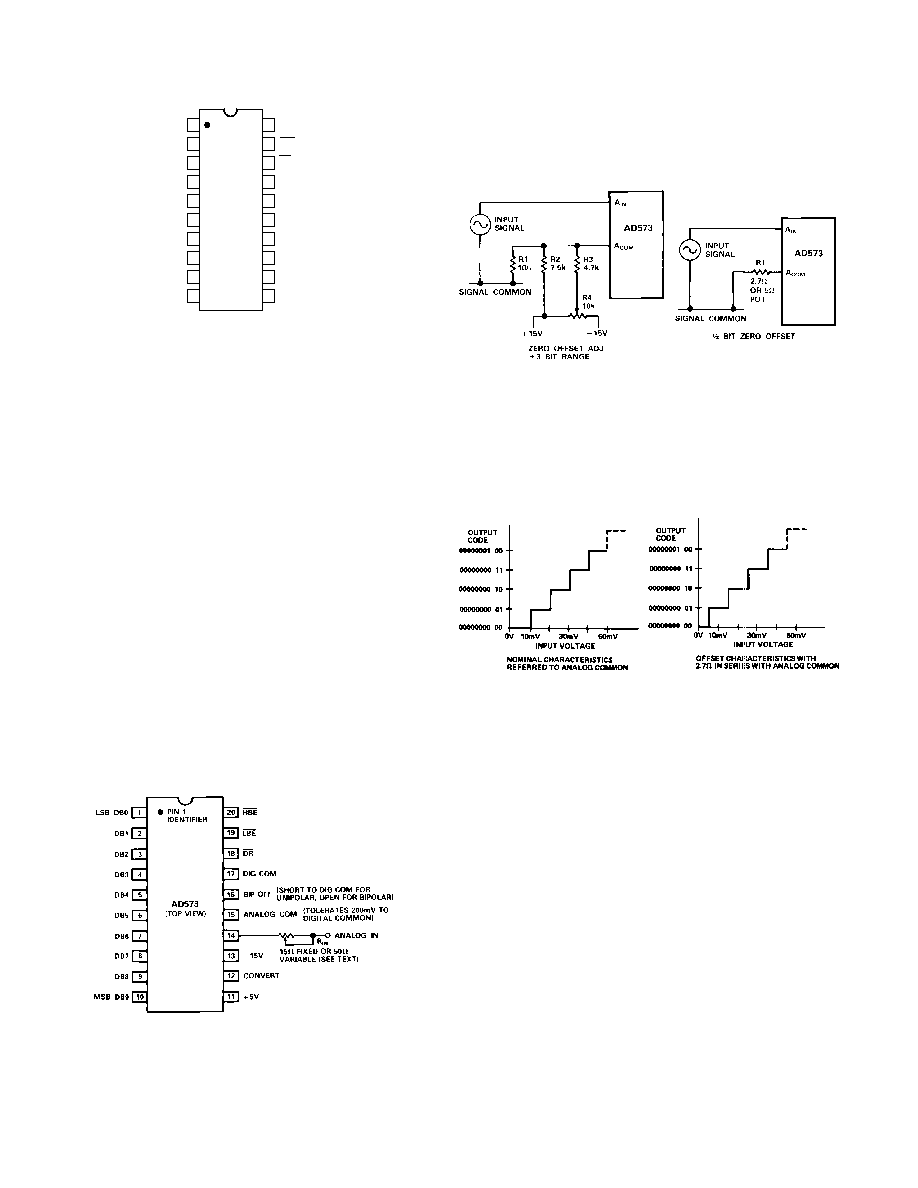
Figure 2. AD573 Pin Connections
Full-Scale Calibration
The 5 k
thin-film input resistor is laser trimmed to produce a
current which matches the full-scale current of the internal
DAC—plus about 0.3%—when an analog input voltage of 9.990
volts (10 volts – 1 LSB) is applied at the input. The input resis-
tor is trimmed in this way so that if a fine trimming potentiom-
eter is inserted in series with the input signal, the input current
at the full-scale input voltage can be trimmed down to match
the DAC full-scale current as precisely as desired. However, for
many applications the nominal 9.99 volt full scale can be
achieved to sufficient accuracy by simply inserting a 15
resis-
tor in series with the analog input to Pin 14. Typical full-scale
calibration error will then be within
±2 LSB or ±0.2%. If more
precise calibration is desired, a 50
trimmer should be used
instead. Set the analog input at 9.990 volts, and set the trimmer
so that the output code is just at the transition between
11111111 10 and 11111111 11. Each LSB will then have a
weight of 9.766 mV. If a nominal full scale of 10.24 volts is de-
sired (which makes the LSB have a weight of exactly 10.00 mV),
a 100
resistor and a 100 trimmer (or a 200 trimmer with
good resolution) should be used. Of course, larger full-scale
ranges can be arranged by using a larger input resistor, but lin-
earity and full-scale temperature coefficient may be compro-
mised if the external resistor becomes a sizeable percentage of
5 k
. Figure 3 illustrates the connections required for full-scale
calibration.
Figure 3. Standard AD573 Connections
Unipolar Offset Calibration
Since the Unipolar Offset is less than
±1 LSB for all versions of
the AD573, most applications will not require trimming. Figure
4 illustrates two trimming methods which can be used if greater
accuracy is necessary.
Figure 4a shows how the converter zero may be offset by up to
±3 bits to correct the device initial offset and/or input signal
offsets. As shown, the circuit gives approximately symmetrical
adjustment in unipolar mode.
Figure 4a.
Figure 4b.
Figure 4. Offset Trims
Figure 5 shows the nominal transfer curve near zero for an
AD573 in unipolar mode. The code transitions are at the edges
of the nominal bit weights. In some applications it will be pref-
erable to offset the code transitions so that they fall between the
nominal bit weights, as shown in the offset characteristics.
Figure 5. AD573 Transfer Curve—Unipolar Operation
(Approximate Bit Weights Shown for Illustration, Nominal
Bit Weights ~ 9.766 mV)
This offset can easily be accomplished as shown in Figure 4b. At
balance (after a conversion) approximately 2 mA flows into the
Analog Common terminal. A 2.7
resistor in series with this
terminal will result in approximately the desired 1/2 bit offset of
the transfer characteristics. The nominal 2 mA Analog Common
current is not closely controlled in manufacture. If high accu-
racy is required, a 5
potentiometer (connected as a rheostat)
can be used as R1. Additional negative offset range may be ob-
tained by using larger values of R1. Of course, if the zero transi-
tion point is changed, the full-scale transition point will also
move. Thus, if an offset of 1/2 LSB is introduced, full-scale
trimming as described on the previous page should be done with
an analog input of 9.985 volts.
NOTE: During a conversion, transient currents from the Analog
Common terminal will disturb the offset voltage. Capacitive
decoupling should not be used around the offset network. These
transients will settle appropriately during a conversion. Capaci-
tive decoupling will “pump up” and fail to settle resulting in
conversion errors. Power supply decoupling, which returns to
analog signal common, should go to the signal input side of the
resistive offset network.
REV. B
相关PDF资料 |
PDF描述 |
|---|---|
| LT1342CG#TR | IC TXRX 5V RS232 3V LOGIC 28SSOP |
| LTC1384IN#PBF | IC TXRX 5V RS232 LOW PWR 18-DIP |
| LTC1384IN | IC TXRX 5V RS232 LOW PWR 18-DIP |
| IDT72231L10PF | IC FIFO SYNC 512X9 10NS 32QFP |
| MS3106A22-12P | CONN PLUG 5POS STRAIGHT W/PINS |
相关代理商/技术参数 |
参数描述 |
|---|---|
| AD573JNZ | 功能描述:IC ADC 10BIT SAR REGISTER 20-DIP RoHS:是 类别:集成电路 (IC) >> 数据采集 - 模数转换器 系列:- 标准包装:1 系列:microPOWER™ 位数:8 采样率(每秒):1M 数据接口:串行,SPI? 转换器数目:1 功率耗散(最大):- 电压电源:模拟和数字 工作温度:-40°C ~ 125°C 安装类型:表面贴装 封装/外壳:24-VFQFN 裸露焊盘 供应商设备封装:24-VQFN 裸露焊盘(4x4) 包装:Digi-Reel® 输入数目和类型:8 个单端,单极 产品目录页面:892 (CN2011-ZH PDF) 其它名称:296-25851-6 |
| AD573JP | 功能描述:IC ADC 10BIT SAR REGISTER 20PLCC RoHS:否 类别:集成电路 (IC) >> 数据采集 - 模数转换器 系列:- 标准包装:1 系列:- 位数:14 采样率(每秒):83k 数据接口:串行,并联 转换器数目:1 功率耗散(最大):95mW 电压电源:双 ± 工作温度:0°C ~ 70°C 安装类型:通孔 封装/外壳:28-DIP(0.600",15.24mm) 供应商设备封装:28-PDIP 包装:管件 输入数目和类型:1 个单端,双极 |
| AD573JPZ | 功能描述:IC ADC 10BIT SAR REGISTER 20PLCC RoHS:是 类别:集成电路 (IC) >> 数据采集 - 模数转换器 系列:- 标准包装:1 系列:- 位数:14 采样率(每秒):83k 数据接口:串行,并联 转换器数目:1 功率耗散(最大):95mW 电压电源:双 ± 工作温度:0°C ~ 70°C 安装类型:通孔 封装/外壳:28-DIP(0.600",15.24mm) 供应商设备封装:28-PDIP 包装:管件 输入数目和类型:1 个单端,双极 |
| AD573KD | 功能描述:IC ADC 10BIT SAR REG 20-CDIP RoHS:否 类别:集成电路 (IC) >> 数据采集 - 模数转换器 系列:- 产品培训模块:Lead (SnPb) Finish for COTS Obsolescence Mitigation Program 标准包装:250 系列:- 位数:12 采样率(每秒):1.8M 数据接口:并联 转换器数目:1 功率耗散(最大):1.82W 电压电源:模拟和数字 工作温度:-40°C ~ 85°C 安装类型:表面贴装 封装/外壳:48-LQFP 供应商设备封装:48-LQFP(7x7) 包装:管件 输入数目和类型:2 个单端,单极 |
| AD573KD/+ | 制造商:Rochester Electronics LLC 功能描述:- Bulk |
发布紧急采购,3分钟左右您将得到回复。