参数资料
| 型号: | AD5760BCPZ |
| 厂商: | Analog Devices Inc |
| 文件页数: | 11/28页 |
| 文件大小: | 0K |
| 描述: | IC DAC VOLT OUT 16BIT 24LFCSP |
| 标准包装: | 1 |
| 设置时间: | 2.5µs |
| 位数: | 16 |
| 数据接口: | DSP,MICROWIRE?,QSPI?,串行,SPI? |
| 转换器数目: | 1 |
| 电压电源: | 模拟和数字,双 ± |
| 工作温度: | -40°C ~ 125°C |
| 安装类型: | 表面贴装 |
| 封装/外壳: | 24-VFQFN 裸露焊盘,CSP |
| 供应商设备封装: | 24-LFCSP-VQ EP(4x5) |
| 包装: | 托盘 |
| 输出数目和类型: | 1 电压,双极 |
第1页第2页第3页第4页第5页第6页第7页第8页第9页第10页当前第11页第12页第13页第14页第15页第16页第17页第18页第19页第20页第21页第22页第23页第24页第25页第26页第27页第28页
Data Sheet
AD5760
Rev. D | Page 19 of 28
THEORY OF OPERATION
The AD5760 is a high accuracy, fast settling, single, 16-bit,
serial input, voltage output DAC. It operates from a VDD supply
voltage of 7.5 V to 16.5 V and a VSS supply of 16.5 V to 2.5 V.
Data is written to the AD5760 in a 24-bit word format via a 3-wire
serial interface. The AD5760 incorporates a power-on reset
circuit that ensures the DAC output powers up to 0 V with the
VOUT pin clamped to AGND through a ~6 kΩ internal resistor.
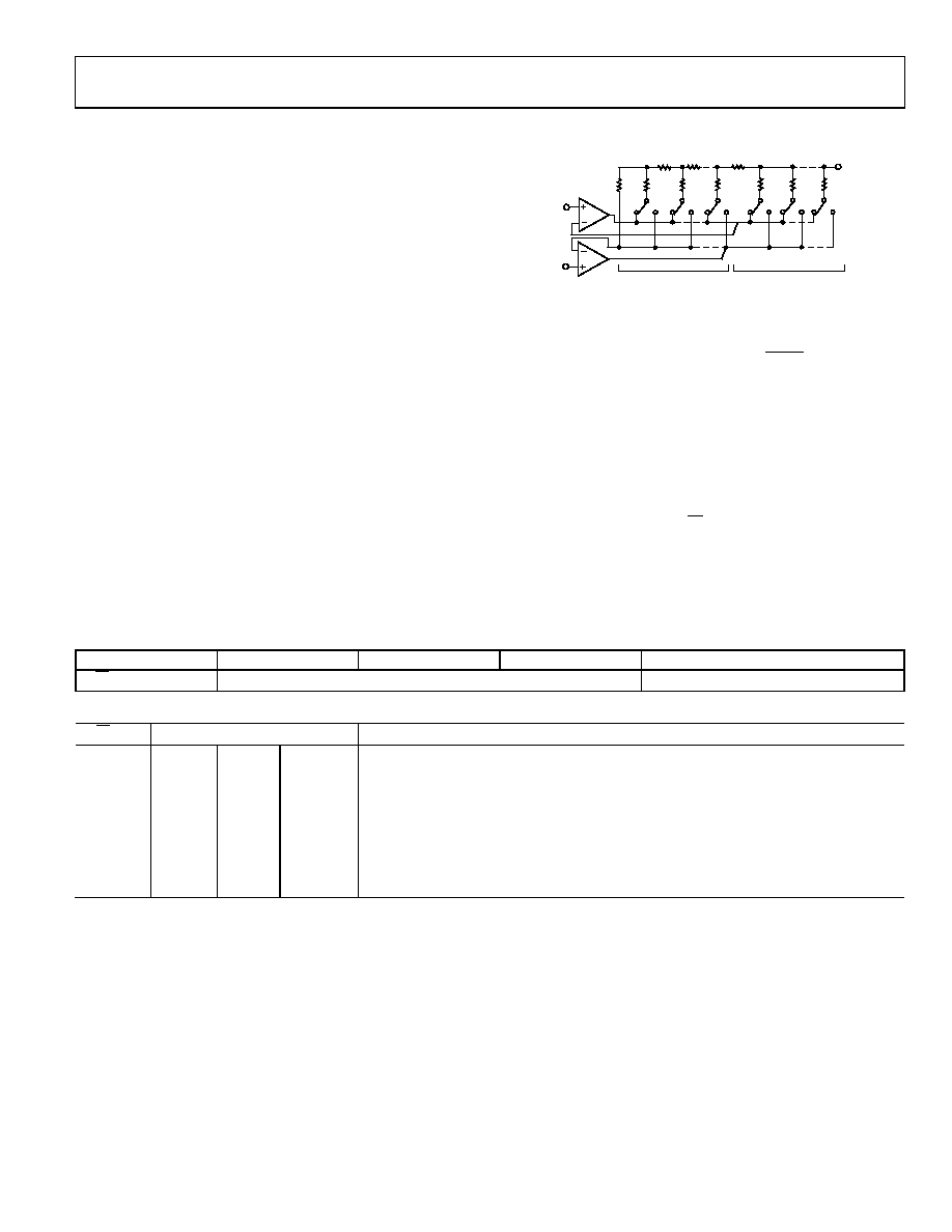
DAC ARCHITECTURE
The architecture of the AD5760 consists of two matched DAC
sections. A simplified circuit diagram is shown in Figure 49.
The six MSBs of the 16-bit data-word are decoded to drive
63 switches, E0 to E62. Each of these switches connects one of
63 matched resistors to either the buffered VREFP or buffered
VREFN voltage. The remaining 10 bits of the data-word drive the
S0 to S9 switches of a 10-bit voltage mode R-2R ladder network.
2R
S0
2R
S1
2R
S9
2R
E62
2R
E61
2R
E0
10-BIT R-2R LADDER
...
RR
R
2R
VOUT
SIX MSBs DECODED INTO
63 EQUAL SEGMENTS
VREFP
VREFN
096
50
-0
50
Figure 49. DAC Ladder Structure Serial Interface
SERIAL INTERFACE
The AD5760 has a 3-wire serial interface (SYNC, SCLK, and
SDIN) that is compatible with SPI, QSPI, and MICROWIRE
interface standards, as well as most DSPs (see Figure 2 for a
timing diagram).
Input Shift Register
The input shift register is 24 bits wide. Data is loaded into the
device MSB first as a 24-bit word under the control of a serial
clock input, SCLK, which can operate at up to 35 MHz. The
input register consists of a R/W bit, three address bits, and
20 data bits as shown in Table 6. The timing diagram for this
operation is shown in Figure 2.
Table 6. Input Shift Register Format
MSB
LSB
DB23
DB22
DB21
DB20
DB19 to DB0
R/W
Register address
Register data
Table 7. Decoding the Input Shift Register
R/W
Register Address
Description
0
No operation (NOP). Used in readback operations.
0
1
Write to the DAC register.
0
1
0
Write to the control register.
0
1
Write to the clearcode register.
0
1
0
Write to the software control register.
1
0
1
Read from the DAC register.
1
0
1
0
Read from the control register.
1
0
1
Read from the clearcode register.
1 X is don’t care.
相关PDF资料 |
PDF描述 |
|---|---|
| AD5762RCSUZ-REEL7 | IC DAC 16BIT QUAD VOUT 32-TQFP |
| AD5763CSUZ-REEL7 | DAC 16BIT DUAL 5V 2LSB 32-TQFP |
| AD5764CSUZ | IC DAC 16BIT QUAD VOUT 32TQFP |
| AD5764RBSUZ | IC DAC 16BIT QUAD VOUT 32-TQFP |
| AD5781BRUZ-REEL7 | IC DAC 18BIT SRL 20TSSOP |
相关代理商/技术参数 |
参数描述 |
|---|---|
| AD5760BCPZ-REEL7 | 功能描述:数模转换器- DAC 16B +/-0.5 LSB INL VOut RoHS:否 制造商:Analog Devices 转换器数量:4 DAC 输出端数量:4 转换速率: 分辨率:12 bit 接口类型:Serial (I2C) 稳定时间: 最大工作温度:+ 105 C 安装风格: 封装 / 箱体:TSSOP 封装:Reel |
| AD5761ACPZ-RL7 | 功能描述:IC DAC 16BIT 1CH 8LSB 16LFCSP 制造商:analog devices inc. 系列:- 零件状态:在售 位数:16 数模转换器数:1 建立时间:12.5μs 输出类型:Voltage - Buffered 差分输出:无 数据接口:SPI 参考类型:外部 电压 - 电源,模拟:4.5 V ~ 30 V, -16.5V 电压 - 电源,数字:1.7 V ~ 5.5 V INL/DNL(LSB):±8(最大),±1(最大) 架构:R-2R 工作温度:-40°C ~ 125°C 标准包装:1 |
| AD5761ARUZ | 功能描述:16 Bit Digital to Analog Converter 1 16-TSSOP 制造商:analog devices inc. 系列:- 包装:管件 零件状态:有效 位数:16 数模转换器数:1 建立时间:12.5μs 输出类型:Voltage - Buffered 差分输出:无 数据接口:SPI 参考类型:外部 电压 - 电源,模拟:4.5 V ~ 30 V, -16.5V 电压 - 电源,数字:1.7 V ~ 5.5 V INL/DNL(LSB):±8(最大),±1(最大) 架构:R-2R 工作温度:-40°C ~ 125°C 封装/外壳:16-TSSOP(0.173",4.40mm 宽) 供应商器件封装:16-TSSOP 标准包装:96 |
| AD5761ARUZ-RL7 | 功能描述:16 Bit Digital to Analog Converter 1 16-TSSOP 制造商:analog devices inc. 系列:- 包装:带卷(TR) 零件状态:有效 位数:16 数模转换器数:1 建立时间:12.5μs 输出类型:Voltage - Buffered 差分输出:无 数据接口:SPI 参考类型:外部 电压 - 电源,模拟:4.5 V ~ 30 V, -16.5V 电压 - 电源,数字:1.7 V ~ 5.5 V INL/DNL(LSB):±8(最大),±1(最大) 架构:R-2R 工作温度:-40°C ~ 125°C 封装/外壳:16-TSSOP(0.173",4.40mm 宽) 供应商器件封装:16-TSSOP 标准包装:1,000 |
| AD5761BCPZ-RL7 | 功能描述:16 Bit Digital to Analog Converter 1 16-LFCSP-WQ (3x3) 制造商:analog devices inc. 系列:- 包装:带卷(TR) 零件状态:有效 位数:16 数模转换器数:1 建立时间:12.5μs 输出类型:Voltage - Buffered 差分输出:无 数据接口:SPI 参考类型:外部 电压 - 电源,模拟:4.5 V ~ 30 V, -16.5V 电压 - 电源,数字:1.7 V ~ 5.5 V INL/DNL(LSB):±2(最大),±1(最大) 架构:R-2R 工作温度:-40°C ~ 125°C 封装/外壳:16-WFQFN 裸露焊盘,CSP 供应商器件封装:16-LFCSP-WQ(3x3) 标准包装:1,500 |
发布紧急采购,3分钟左右您将得到回复。