参数资料
| 型号: | AD5760BCPZ |
| 厂商: | Analog Devices Inc |
| 文件页数: | 17/28页 |
| 文件大小: | 0K |
| 描述: | IC DAC VOLT OUT 16BIT 24LFCSP |
| 标准包装: | 1 |
| 设置时间: | 2.5µs |
| 位数: | 16 |
| 数据接口: | DSP,MICROWIRE?,QSPI?,串行,SPI? |
| 转换器数目: | 1 |
| 电压电源: | 模拟和数字,双 ± |
| 工作温度: | -40°C ~ 125°C |
| 安装类型: | 表面贴装 |
| 封装/外壳: | 24-VFQFN 裸露焊盘,CSP |
| 供应商设备封装: | 24-LFCSP-VQ EP(4x5) |
| 包装: | 托盘 |
| 输出数目和类型: | 1 电压,双极 |
第1页第2页第3页第4页第5页第6页第7页第8页第9页第10页第11页第12页第13页第14页第15页第16页当前第17页第18页第19页第20页第21页第22页第23页第24页第25页第26页第27页第28页
AD5760
Data Sheet
Rev. D | Page 24 of 28
AD5760 FEATURES
POWER-ON TO 0 V
The AD5760 contains a power-on reset circuit that, as well as
resetting all registers to their default values, controls the output
voltage during power-up. Upon power-on, the DAC is placed in
tristate (its reference inputs are disconnected), and its output is
clamped to AGND through a ~6 k resistor. The DAC remains
in this state until programmed otherwise via the control register.
This is a useful feature in applications where it is important to
know the state of the DAC output while it is in the process of
powering up.
CONFIGURING THE AD5760
After power-on, the AD5760 must be configured to put it into
normal operating mode before programming the output. To
do this, the control register must be programmed. The DAC
is removed from tristate by clearing the DACTRI bit, and the
output clamp is removed by clearing the OPGND bit. At this
point, the output goes to VREFN unless an alternative value is
first programmed to the DAC register.
DAC OUTPUT STATE
The DAC output can be placed in one of three states, controlled
by the DACTRI and OPGND bits of the control register, as
shown in Table 15.
Table 15. Output State Truth Table
DACTRI
OPGND
Output State
0
Normal operating mode.
0
1
Output is clamped via ~6 k to AGND.
1
0
Output is in tristate.
1
Output is clamped via ~6 k to AGND.
OUTPUT AMPLIFIER CONFIGURATION
There are a number of different ways that an output amplifier
can be connected to the AD5760, depending on the voltage
references applied and the desired output voltage span.
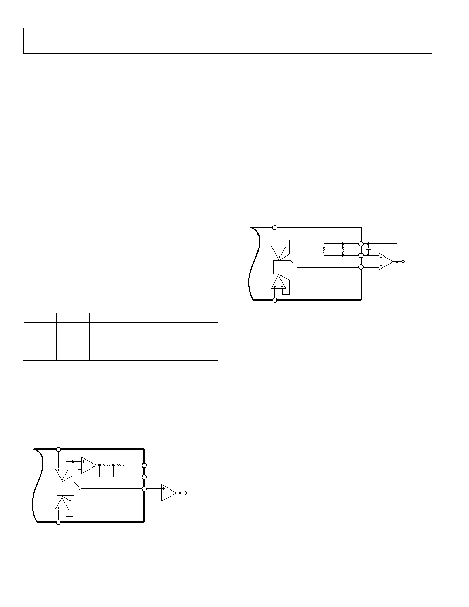
Unity-Gain Configuration
Figure 50 shows an output amplifier configured for unity gain.
In this configuration, the output spans from VREFN to VREFP.
A1
6.8k 6.8k
R1
RFB
VREFP
RFB
INV
VOUT
16-BIT
DAC
VREFN
AD5760
AD8675
ADA4898-1
ADA4004-1
09650-
052
Figure 50. Output Amplifier in Unity-Gain Configuration
A second unity-gain configuration for the output amplifier is
one that removes an offset from the input bias currents of the
amplifier. It does this by inserting a resistance in the feedback
path of the amplifier that is equal to the output resistance of the
DAC. The DAC output resistance is 3.4 k. By connecting R1
and RFB in parallel, a resistance equal to the DAC resistance is
available on chip. Because the resistors are all on one piece of
silicon, they are temperature coefficient matched. To enable this
mode of operation, the RBUF bit of the control register must be
set to Logic 1. Figure 51 shows how the output amplifier is
connected to the AD5760. In this configuration, the output
amplifier is in unity gain, and the output spans from VREFN to
VREFP. This unity-gain configuration allows a capacitor to be
placed in the amplifier feedback path to improve dynamic
performance.
VREFP
RFB
INV
VOUT
10pF
16-BIT
DAC
VREFN
AD5760
AD8675
ADA4898-1
ADA4004-1
RFB
6.8k
R1
6.8k
09650-
053
Figure 51. Output Amplifier in Unity-Gain with Amplifier Input Bias Current
Compensation
相关PDF资料 |
PDF描述 |
|---|---|
| AD5762RCSUZ-REEL7 | IC DAC 16BIT QUAD VOUT 32-TQFP |
| AD5763CSUZ-REEL7 | DAC 16BIT DUAL 5V 2LSB 32-TQFP |
| AD5764CSUZ | IC DAC 16BIT QUAD VOUT 32TQFP |
| AD5764RBSUZ | IC DAC 16BIT QUAD VOUT 32-TQFP |
| AD5781BRUZ-REEL7 | IC DAC 18BIT SRL 20TSSOP |
相关代理商/技术参数 |
参数描述 |
|---|---|
| AD5760BCPZ-REEL7 | 功能描述:数模转换器- DAC 16B +/-0.5 LSB INL VOut RoHS:否 制造商:Analog Devices 转换器数量:4 DAC 输出端数量:4 转换速率: 分辨率:12 bit 接口类型:Serial (I2C) 稳定时间: 最大工作温度:+ 105 C 安装风格: 封装 / 箱体:TSSOP 封装:Reel |
| AD5761ACPZ-RL7 | 功能描述:IC DAC 16BIT 1CH 8LSB 16LFCSP 制造商:analog devices inc. 系列:- 零件状态:在售 位数:16 数模转换器数:1 建立时间:12.5μs 输出类型:Voltage - Buffered 差分输出:无 数据接口:SPI 参考类型:外部 电压 - 电源,模拟:4.5 V ~ 30 V, -16.5V 电压 - 电源,数字:1.7 V ~ 5.5 V INL/DNL(LSB):±8(最大),±1(最大) 架构:R-2R 工作温度:-40°C ~ 125°C 标准包装:1 |
| AD5761ARUZ | 功能描述:16 Bit Digital to Analog Converter 1 16-TSSOP 制造商:analog devices inc. 系列:- 包装:管件 零件状态:有效 位数:16 数模转换器数:1 建立时间:12.5μs 输出类型:Voltage - Buffered 差分输出:无 数据接口:SPI 参考类型:外部 电压 - 电源,模拟:4.5 V ~ 30 V, -16.5V 电压 - 电源,数字:1.7 V ~ 5.5 V INL/DNL(LSB):±8(最大),±1(最大) 架构:R-2R 工作温度:-40°C ~ 125°C 封装/外壳:16-TSSOP(0.173",4.40mm 宽) 供应商器件封装:16-TSSOP 标准包装:96 |
| AD5761ARUZ-RL7 | 功能描述:16 Bit Digital to Analog Converter 1 16-TSSOP 制造商:analog devices inc. 系列:- 包装:带卷(TR) 零件状态:有效 位数:16 数模转换器数:1 建立时间:12.5μs 输出类型:Voltage - Buffered 差分输出:无 数据接口:SPI 参考类型:外部 电压 - 电源,模拟:4.5 V ~ 30 V, -16.5V 电压 - 电源,数字:1.7 V ~ 5.5 V INL/DNL(LSB):±8(最大),±1(最大) 架构:R-2R 工作温度:-40°C ~ 125°C 封装/外壳:16-TSSOP(0.173",4.40mm 宽) 供应商器件封装:16-TSSOP 标准包装:1,000 |
| AD5761BCPZ-RL7 | 功能描述:16 Bit Digital to Analog Converter 1 16-LFCSP-WQ (3x3) 制造商:analog devices inc. 系列:- 包装:带卷(TR) 零件状态:有效 位数:16 数模转换器数:1 建立时间:12.5μs 输出类型:Voltage - Buffered 差分输出:无 数据接口:SPI 参考类型:外部 电压 - 电源,模拟:4.5 V ~ 30 V, -16.5V 电压 - 电源,数字:1.7 V ~ 5.5 V INL/DNL(LSB):±2(最大),±1(最大) 架构:R-2R 工作温度:-40°C ~ 125°C 封装/外壳:16-WFQFN 裸露焊盘,CSP 供应商器件封装:16-LFCSP-WQ(3x3) 标准包装:1,500 |
发布紧急采购,3分钟左右您将得到回复。