- 您现在的位置:买卖IC网 > PDF目录1979 > AD5763CSUZ-REEL7 (Analog Devices Inc)DAC 16BIT DUAL 5V 2LSB 32-TQFP PDF资料下载
参数资料
| 型号: | AD5763CSUZ-REEL7 |
| 厂商: | Analog Devices Inc |
| 文件页数: | 16/28页 |
| 文件大小: | 0K |
| 描述: | DAC 16BIT DUAL 5V 2LSB 32-TQFP |
| 产品培训模块: | Data Converter Fundamentals DAC Architectures |
| 产品变化通告: | AD5763/65 Metal Layer Edit Change 08/Sept/2009 |
| 设计资源: | High Accuracy, Bipolar Voltage Output Digital-to-Analog Conversion Using AD5763 (CN0074) |
| 标准包装: | 500 |
| 设置时间: | 8µs |
| 位数: | 16 |
| 数据接口: | 串行 |
| 转换器数目: | 2 |
| 电压电源: | 双 ± |
| 功率耗散(最大): | 45mW |
| 工作温度: | -40°C ~ 105°C |
| 安装类型: | 表面贴装 |
| 封装/外壳: | 32-TQFP |
| 供应商设备封装: | 32-TQFP(7x7) |
| 包装: | 带卷 (TR) |
| 输出数目和类型: | 2 电压,双极 |
| 采样率(每秒): | * |
第1页第2页第3页第4页第5页第6页第7页第8页第9页第10页第11页第12页第13页第14页第15页当前第16页第17页第18页第19页第20页第21页第22页第23页第24页第25页第26页第27页第28页
Data Sheet
AD5763
Rev. C | Page 23 of 28
LOCAL GROUND OFFSET ADJUST
The AD5763 incorporates a local-ground-offset adjust feature
which, when enabled in the function register, adjusts the DAC
outputs for voltage differences between the individual DAC
ground pins and the REFGND pin ensuring that the DAC
output voltages are always with respect to the local DAC
ground pin. For instance, if Pin AGNDA is at 5 mV with
respect to the REFGND pin and VOUTA is measured with
respect to AGNDA, then a 5 mV error results, enabling the
local-ground-offset adjust feature which adjusts VOUTA by
+5 mV, eliminating the error.
POWER-ON STATUS
The AD5763 has multiple power supply and digital input pins.
It is important to consider the sequence in which the pins are
powered up to ensure the AD5763 powers-on in the required
state. The outputs will power-on either clamped to AGNDx,
driving 0 V, or driving negative full-scale output (4.096 V)
depending on how the BIN/2sCOMP, CLR, and LDAC pins
are configured during power-up. If the CLR pin is connected to
DGND, it causes the DAC registers to be loaded with 0x0000
and the outputs to be updated. Consequently, the outputs are
loaded with 0 V if BIN/2sCOMP is connected to DGND or
negative full-scale (4.096 V) if BIN/2sCOMP is connected to
DVCC corresponding respectively to the twos complement and
binary voltages for the digital code 0x0000. During power-up
the state of the LDAC pin has an identical effect to that of the
CLR pin. If both the CLR and LDAC pins are connected to
DVCC during power-up the outputs power-on clamped to
AGNDx and remain so until a valid write is made to the device.
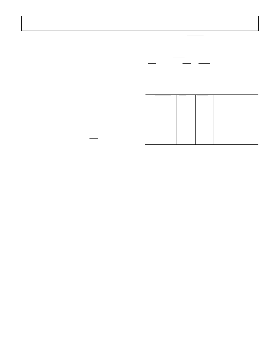
outlines the possible output power-on states.
Table 19. Output Power-On State
BIN/2sCOMP
CLR
LDAC
VOUT at Power-On
DGND
0 V
DGND
DVCC
0 V
DGND
DVCC
DGND
0 V
DGND
DVCC
Clamped to AGNDx
DVCC
DGND
4.096 V
DVCC
DGND
DVCC
4.096 V
DVCC
DGND
4.096 V
DVCC
Clamped to AGNDx
相关PDF资料 |
PDF描述 |
|---|---|
| AD5764CSUZ | IC DAC 16BIT QUAD VOUT 32TQFP |
| AD5764RBSUZ | IC DAC 16BIT QUAD VOUT 32-TQFP |
| AD5781BRUZ-REEL7 | IC DAC 18BIT SRL 20TSSOP |
| AD5790BCPZ | IC DAC VOLT OUT 20BIT 24LFCSP |
| AD5791BRUZ | IC DAC 20BIT SRL 20TSSOP |
相关代理商/技术参数 |
参数描述 |
|---|---|
| AD5763CSUZ-TR | 制造商:Analog Devices 功能描述:16BIT +/-5V DUAL 1LSB - Tape and Reel |
| AD5764 | 制造商:AD 制造商全称:Analog Devices 功能描述:Complete, Quad, 14/16-Bit, High Accuracy, Serial Input, Bipolar Voltage Output DAC |
| AD5764ASU | 制造商:AD 制造商全称:Analog Devices 功能描述:Complete, Quad, 14/16-Bit, High Accuracy, Serial Input, Bipolar Voltage Output DAC |
| AD5764ASUZ | 功能描述:IC DAC 16BIT QUAD VOUT 32-TQFP RoHS:是 类别:集成电路 (IC) >> 数据采集 - 数模转换器 系列:- 产品培训模块:Lead (SnPb) Finish for COTS Obsolescence Mitigation Program 标准包装:50 系列:- 设置时间:4µs 位数:12 数据接口:串行 转换器数目:2 电压电源:单电源 功率耗散(最大):- 工作温度:-40°C ~ 85°C 安装类型:表面贴装 封装/外壳:8-TSSOP,8-MSOP(0.118",3.00mm 宽) 供应商设备封装:8-uMAX 包装:管件 输出数目和类型:2 电压,单极 采样率(每秒):* 产品目录页面:1398 (CN2011-ZH PDF) |
| AD5764ASUZ-REEL7 | 功能描述:IC DAC 16BIT QUAD VOUT 32-TQFP RoHS:是 类别:集成电路 (IC) >> 数据采集 - 数模转换器 系列:- 产品培训模块:Data Converter Fundamentals DAC Architectures 标准包装:750 系列:- 设置时间:7µs 位数:16 数据接口:并联 转换器数目:1 电压电源:双 ± 功率耗散(最大):100mW 工作温度:0°C ~ 70°C 安装类型:表面贴装 封装/外壳:28-LCC(J 形引线) 供应商设备封装:28-PLCC(11.51x11.51) 包装:带卷 (TR) 输出数目和类型:1 电压,单极;1 电压,双极 采样率(每秒):143k |
发布紧急采购,3分钟左右您将得到回复。