- 您现在的位置:买卖IC网 > PDF目录1979 > AD5763CSUZ-REEL7 (Analog Devices Inc)DAC 16BIT DUAL 5V 2LSB 32-TQFP PDF资料下载
参数资料
| 型号: | AD5763CSUZ-REEL7 |
| 厂商: | Analog Devices Inc |
| 文件页数: | 2/28页 |
| 文件大小: | 0K |
| 描述: | DAC 16BIT DUAL 5V 2LSB 32-TQFP |
| 产品培训模块: | Data Converter Fundamentals DAC Architectures |
| 产品变化通告: | AD5763/65 Metal Layer Edit Change 08/Sept/2009 |
| 设计资源: | High Accuracy, Bipolar Voltage Output Digital-to-Analog Conversion Using AD5763 (CN0074) |
| 标准包装: | 500 |
| 设置时间: | 8µs |
| 位数: | 16 |
| 数据接口: | 串行 |
| 转换器数目: | 2 |
| 电压电源: | 双 ± |
| 功率耗散(最大): | 45mW |
| 工作温度: | -40°C ~ 105°C |
| 安装类型: | 表面贴装 |
| 封装/外壳: | 32-TQFP |
| 供应商设备封装: | 32-TQFP(7x7) |
| 包装: | 带卷 (TR) |
| 输出数目和类型: | 2 电压,双极 |
| 采样率(每秒): | * |
第1页当前第2页第3页第4页第5页第6页第7页第8页第9页第10页第11页第12页第13页第14页第15页第16页第17页第18页第19页第20页第21页第22页第23页第24页第25页第26页第27页第28页
AD5763
Data Sheet
Rev. C | Page 10 of 29
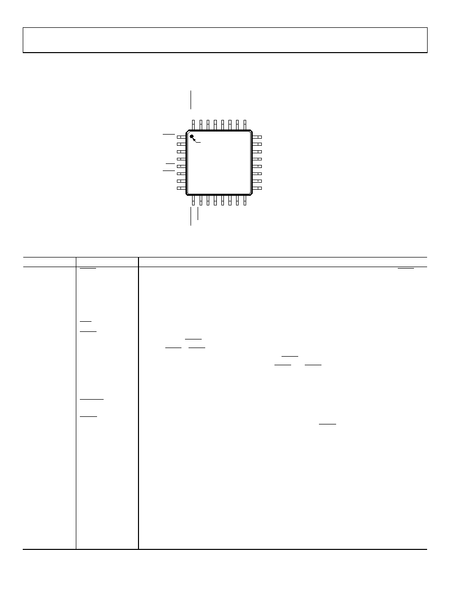
PIN CONFIGURATION AND FUNCTION DESCRIPTIONS
1
32
25
916
8
24
17
PIN 1
INDICATOR
AD5763
TOP VIEW
(Not to scale)
NC = NO CONNECT
SYNC
SCLK
SDIN
SDO
CLR
LDAC
D0
D1
NC
VOUTA
AGNDA
AGNDB
VOUTB
NC
BI
N/
2sCO
M
P
AV
DD
AV
SS
TE
M
P
RE
F
G
ND
NC
RE
F
B
RE
F
A
RS
T
O
UT
RS
T
IN
DG
N
D
DV
CC
AV
DD
PG
N
D
AV
SS
IS
C
0
72
50
-00
6
Figure 6. Pin Configuration
Table 6. Pin Function Descriptions
Pin No.
Mnemonic
Description
1
SYNC
Active Low Input. This pin is the frame synchronization signal for the serial interface. While SYNC is
low, data is transferred in on the falling edge of SCLK.
2
SCLK
Serial Clock Input. Data is clocked into the shift register on the falling edge of SCLK. This pin
operates at clock speeds up to 30 MHz.
3
SDIN
Serial Data Input. Data must be valid on the falling edge of SCLK.
4
SDO
Serial Data Output. Used to clock data from the serial register in daisy-chain or readback mode.
51
CLR
Negative Edge Triggered Input. Asserting this pin sets the DAC registers to 0x0000.1
6
LDAC
Load DAC. Logic input. This pin is used to update the DAC registers and consequently the analog
outputs. When LDAC is tied permanently low, the addressed DAC register is updated on the rising
edge of SYNC. If LDAC is held high during the write cycle, the DAC input register is updated but the
output update is held off until the falling edge of LDAC. In this mode, all analog outputs can be
updated simultaneously on the falling edge of LDAC. The LDAC pin must not be left unconnected.
7, 8
D0, D1
D0 and D1 form a digital I/O port. The user can set up these pins as inputs or outputs that are confi-
gurable and readable over the serial interface. When configured as inputs, these pins have weak
internal pull-ups to DVCC. When programmed as outputs, D0 and D1 are referenced by DVCC and DGND.
9
RSTOUT
Reset Logic Output. This pin is the output from the on-chip voltage monitor used in the reset
circuit. If desired, it can be used to control other system components.
10
RSTIN
Reset Logic Input. This input allows external access to the internal reset logic. Applying a Logic 0 to
this input clamps the DAC outputs to 0 V. In normal operation, RSTIN should be tied to Logic 1.
Register values remain unchanged.
11
DGND
Digital Ground Pin.
12
DVCC
Digital Supply Pin. The voltage ranges from 2.7 V to 5.25 V.
13, 31
AVDD
Positive Analog Supply Pins. The voltage ranges from 4.75 V to 5.25 V.
14
PGND
Ground Reference Point for Analog Circuitry.
15, 30
AVSS
Negative Analog Supply Pins. The voltage ranges from –5.25 V to –4.75 V.
16
ISCC
This pin is used in association with an optional external resistor connected to AGND and programs
the short-circuit current of the output amplifiers. See the Design Features section for further details.
17, 18, 23, 24, 27
NC
No Connect.
19
VOUTB
Analog Output Voltage of DAC B. Buffered output with a nominal full-scale output range of ±4.096 V. The
output amplifier is capable of directly driving a 5 kΩ, 200 pF load.
20
AGNDB
Ground Reference Pin for the DAC B Output Amplifier.
21
AGNDA
Ground Reference Pin for the DAC A Output Amplifier.
相关PDF资料 |
PDF描述 |
|---|---|
| AD5764CSUZ | IC DAC 16BIT QUAD VOUT 32TQFP |
| AD5764RBSUZ | IC DAC 16BIT QUAD VOUT 32-TQFP |
| AD5781BRUZ-REEL7 | IC DAC 18BIT SRL 20TSSOP |
| AD5790BCPZ | IC DAC VOLT OUT 20BIT 24LFCSP |
| AD5791BRUZ | IC DAC 20BIT SRL 20TSSOP |
相关代理商/技术参数 |
参数描述 |
|---|---|
| AD5763CSUZ-TR | 制造商:Analog Devices 功能描述:16BIT +/-5V DUAL 1LSB - Tape and Reel |
| AD5764 | 制造商:AD 制造商全称:Analog Devices 功能描述:Complete, Quad, 14/16-Bit, High Accuracy, Serial Input, Bipolar Voltage Output DAC |
| AD5764ASU | 制造商:AD 制造商全称:Analog Devices 功能描述:Complete, Quad, 14/16-Bit, High Accuracy, Serial Input, Bipolar Voltage Output DAC |
| AD5764ASUZ | 功能描述:IC DAC 16BIT QUAD VOUT 32-TQFP RoHS:是 类别:集成电路 (IC) >> 数据采集 - 数模转换器 系列:- 产品培训模块:Lead (SnPb) Finish for COTS Obsolescence Mitigation Program 标准包装:50 系列:- 设置时间:4µs 位数:12 数据接口:串行 转换器数目:2 电压电源:单电源 功率耗散(最大):- 工作温度:-40°C ~ 85°C 安装类型:表面贴装 封装/外壳:8-TSSOP,8-MSOP(0.118",3.00mm 宽) 供应商设备封装:8-uMAX 包装:管件 输出数目和类型:2 电压,单极 采样率(每秒):* 产品目录页面:1398 (CN2011-ZH PDF) |
| AD5764ASUZ-REEL7 | 功能描述:IC DAC 16BIT QUAD VOUT 32-TQFP RoHS:是 类别:集成电路 (IC) >> 数据采集 - 数模转换器 系列:- 产品培训模块:Data Converter Fundamentals DAC Architectures 标准包装:750 系列:- 设置时间:7µs 位数:16 数据接口:并联 转换器数目:1 电压电源:双 ± 功率耗散(最大):100mW 工作温度:0°C ~ 70°C 安装类型:表面贴装 封装/外壳:28-LCC(J 形引线) 供应商设备封装:28-PLCC(11.51x11.51) 包装:带卷 (TR) 输出数目和类型:1 电压,单极;1 电压,双极 采样率(每秒):143k |
发布紧急采购,3分钟左右您将得到回复。