参数资料
| 型号: | AD5764CSUZ |
| 厂商: | Analog Devices Inc |
| 文件页数: | 11/28页 |
| 文件大小: | 0K |
| 描述: | IC DAC 16BIT QUAD VOUT 32TQFP |
| 产品培训模块: | Data Converter Fundamentals DAC Architectures |
| 产品变化通告: | AD5764(R), AD5744R Product Change 04/Sept/2009 |
| 设计资源: | High Accuracy, Bipolar Voltage Output Digital-to-Analog Conversion Using AD5764 (CN0006) |
| 标准包装: | 1 |
| 设置时间: | 8µs |
| 位数: | 16 |
| 数据接口: | 串行 |
| 转换器数目: | 4 |
| 电压电源: | 双 ± |
| 功率耗散(最大): | 275 mW |
| 工作温度: | -40°C ~ 85°C |
| 安装类型: | 表面贴装 |
| 封装/外壳: | 32-TQFP |
| 供应商设备封装: | 32-TQFP(7x7) |
| 包装: | 托盘 |
| 输出数目和类型: | 4 电压,双极 |
| 采样率(每秒): | 1.26M |
| 产品目录页面: | 784 (CN2011-ZH PDF) |
| 配用: | EVAL-AD5764EBZ-ND - BOARD EVAL FOR AD5764 |
第1页第2页第3页第4页第5页第6页第7页第8页第9页第10页当前第11页第12页第13页第14页第15页第16页第17页第18页第19页第20页第21页第22页第23页第24页第25页第26页第27页第28页
Data Sheet
AD5764
Rev. F | Page 19 of 28
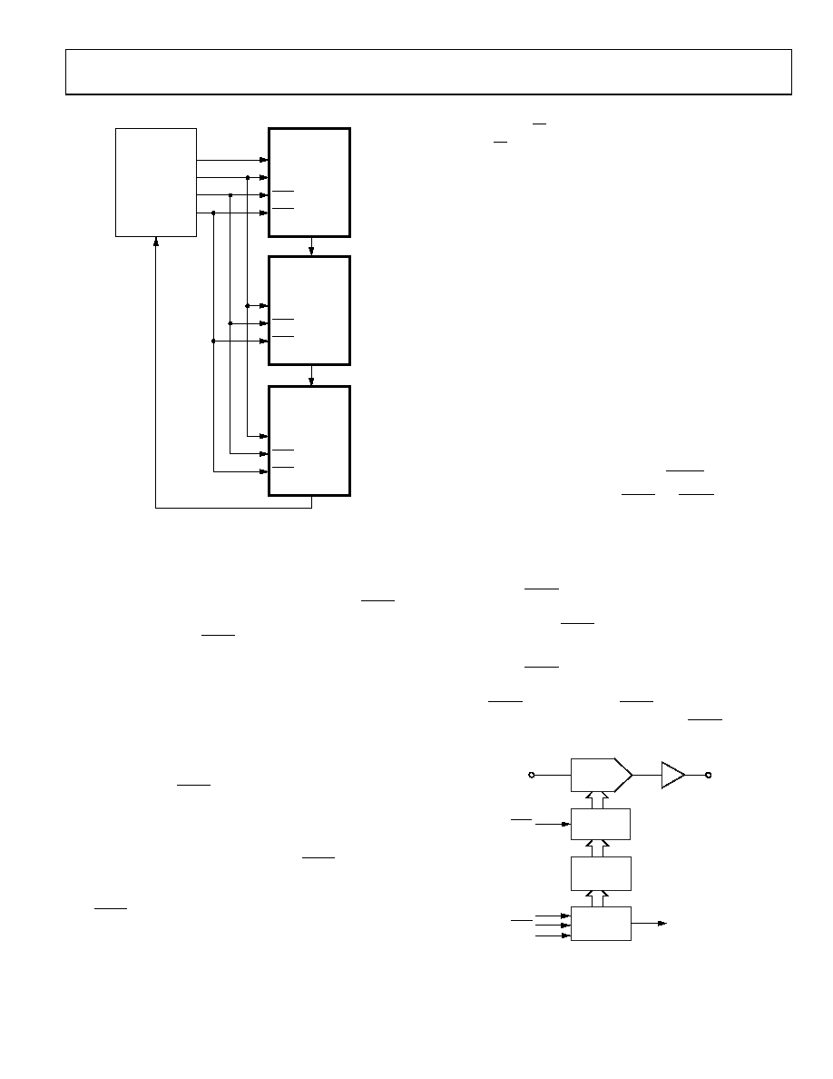
Daisy-Chain Operation
05
30
3-
06
1
68HC111
MISO
SYNC
SDIN
SCLK
MOSI
SCK
PC7
PC6
LDAC
SDO
SYNC
SCLK
LDAC
SDO
SYNC
SCLK
LDAC
SDO
SDIN
1ADDITIONAL PINS OMITTED FOR CLARITY
AD57641
Figure 33. Daisy-Chaining the AD5764
For systems that contain several devices, the SDO pin can be
used to daisy-chain several devices together. This daisy-chain
mode can be useful in system diagnostics and in reducing the
number of serial interface lines. The first falling edge of SYNC
starts the write cycle. The SCLK is continuously applied to the
input shift register when SYNC is low. If more than 24 clock
pulses are applied, the data ripples out of the input shift register
and appears on the SDO line. This data is clocked out on the
rising edge of SCLK and is valid on the falling edge. By connect-
ing the SDO of the first device to the SDIN input of the next device
in the chain, a multidevice interface is constructed. Each device in
the system requires 24 clock pulses. Therefore, the total number of
clock cycles must equal 24N, where N is the total number of
AD5764 devices in the chain. When the serial transfer to all
devices is complete, SYNC is taken high. This latches the input
data in each device in the daisy chain and prevents any further
data from being clocked into the input shift register. The serial
clock can be a continuous or a gated clock.
A continuous SCLK source can only be used if SYNC is held low
for the correct number of clock cycles. In gated clock mode, a burst
clock containing the exact number of clock cycles must be used,
and SYNC must be taken high after the final clock to latch the data.
Readback Operation
Before a readback operation is initiated, the SDO pin must be
enabled by writing to the function register and clearing the SDO
disable bit; this bit is cleared by default. Readback mode is invoked
by setting the R/W bit = 1 in the serial input shift register write.
With R/W = 1, Bit A2 to Bit A0, in association with Bit REG2,
Bit REG1, and Bit REG0, select the register to be read. The
remaining data bits in the write sequence are don’t cares. During
the next SPI write, the data appearing on the SDO output
contain the data from the previously addressed register. For a
read of a single register, the NOP command can be used in
clocking out the data from the selected register on SDO. The
readback diagram in
shows the readback sequence. For
example, to read back the fine gain register of Channel A on the
AD5764, implement the following:
1.
Write 0xA0XXXX to the AD5764 input shift register. This
configures the AD5764 for read mode with the fine gain
register of Channel A selected. Note that all the data bits,
DB15 to DB0, are don’t cares.
2.
Follow this with a second write, an NOP condition,
0x00XXXX. During this write, the data from the fine gain
register is clocked out on the SDO line, that is, data clocked
out contain the data from the fine gain register in Bit DB5
to Bit DB0.
SIMULTANEOUS UPDATING VIA LDAC
Depending on the status of both SYNC and LDAC, and after
data has been transferred into the input register of the DACs,
there are two ways in which the data register and DAC outputs
can be updated.
Individual DAC Updating
In this mode, LDAC is held low while data is being clocked into
the input shift register. The addressed DAC output is updated
on the rising edge of SYNC.
Simultaneous Updating of All DACs
In this mode, LDAC is held high while data is being clocked
into the input shift register. All DAC outputs are updated by
taking LDAC low any time after SYNC has been taken high.
The update now occurs on the falling edge of LDAC.
VOUTx
DATA
REGISTER
INTERFACE
LOGIC
OUTPUT
I/V AMPLIFIER
LDAC
SDO
SDIN
16-BIT
DAC
VREFIN
SYNC
INPUT
REGISTER
SCLK
05
30
3-
0
62
Figure 34. Simplified Serial Interface of Input Loading Circuitry
for One DAC Channel
相关PDF资料 |
PDF描述 |
|---|---|
| AD5764RBSUZ | IC DAC 16BIT QUAD VOUT 32-TQFP |
| AD5781BRUZ-REEL7 | IC DAC 18BIT SRL 20TSSOP |
| AD5790BCPZ | IC DAC VOLT OUT 20BIT 24LFCSP |
| AD5791BRUZ | IC DAC 20BIT SRL 20TSSOP |
| AD5821ABCBZ-REEL | IC DAC 10BIT CURRENTSINK 9WLCSP |
相关代理商/技术参数 |
参数描述 |
|---|---|
| AD5764CSUZ-REEL7 | 功能描述:IC DAC 16BIT QUAD BIPO 32-TQFP RoHS:是 类别:集成电路 (IC) >> 数据采集 - 数模转换器 系列:- 产品培训模块:Lead (SnPb) Finish for COTS Obsolescence Mitigation Program 标准包装:1,000 系列:- 设置时间:1µs 位数:8 数据接口:串行 转换器数目:8 电压电源:双 ± 功率耗散(最大):941mW 工作温度:0°C ~ 70°C 安装类型:表面贴装 封装/外壳:24-SOIC(0.295",7.50mm 宽) 供应商设备封装:24-SOIC W 包装:带卷 (TR) 输出数目和类型:8 电压,单极 采样率(每秒):* |
| AD5764R | 制造商:AD 制造商全称:Analog Devices 功能描述:Complete Quad, 16-Bit, High Accuracy, Serial Input, Bipolar Voltage Output DAC |
| AD5764R_08 | 制造商:AD 制造商全称:Analog Devices 功能描述:Complete Quad, 16-Bit, High Accuracy, Serial Input, Bipolar Voltage Output DAC |
| AD5764RASUZ | 制造商:AD 制造商全称:Analog Devices 功能描述:Complete Quad, 16-Bit, High Accuracy, Serial Input, Bipolar Voltage Output DAC |
| AD5764RASUZ-REEL7 | 制造商:AD 制造商全称:Analog Devices 功能描述:Complete Quad, 16-Bit, High Accuracy, Serial Input, Bipolar Voltage Output DAC |
发布紧急采购,3分钟左右您将得到回复。