参数资料
| 型号: | AD5764RCSUZ |
| 厂商: | Analog Devices Inc |
| 文件页数: | 16/32页 |
| 文件大小: | 0K |
| 描述: | IC DAC QUAD 16BIT VOUT 32-TQFP |
| 产品培训模块: | Data Converter Fundamentals DAC Architectures |
| 产品变化通告: | AD5764(R), AD5744R Product Change 04/Sept/2009 |
| 设计资源: | High Accuracy, Bipolar Voltage Output Digital-to-Analog Conversion Using AD5764 (CN0006) |
| 标准包装: | 1 |
| 设置时间: | 8µs |
| 位数: | 16 |
| 数据接口: | DSP,MICROWIRE?,QSPI?,串行,SPI? |
| 转换器数目: | 4 |
| 电压电源: | 双 ± |
| 功率耗散(最大): | 275 mW |
| 工作温度: | -40°C ~ 85°C |
| 安装类型: | 表面贴装 |
| 封装/外壳: | 32-TQFP |
| 供应商设备封装: | 32-TQFP(7x7) |
| 包装: | 托盘 |
| 输出数目和类型: | 4 电压,双极 |
第1页第2页第3页第4页第5页第6页第7页第8页第9页第10页第11页第12页第13页第14页第15页当前第16页第17页第18页第19页第20页第21页第22页第23页第24页第25页第26页第27页第28页第29页第30页第31页第32页
Data Sheet
AD5764R
Rev. D | Page 23 of 32
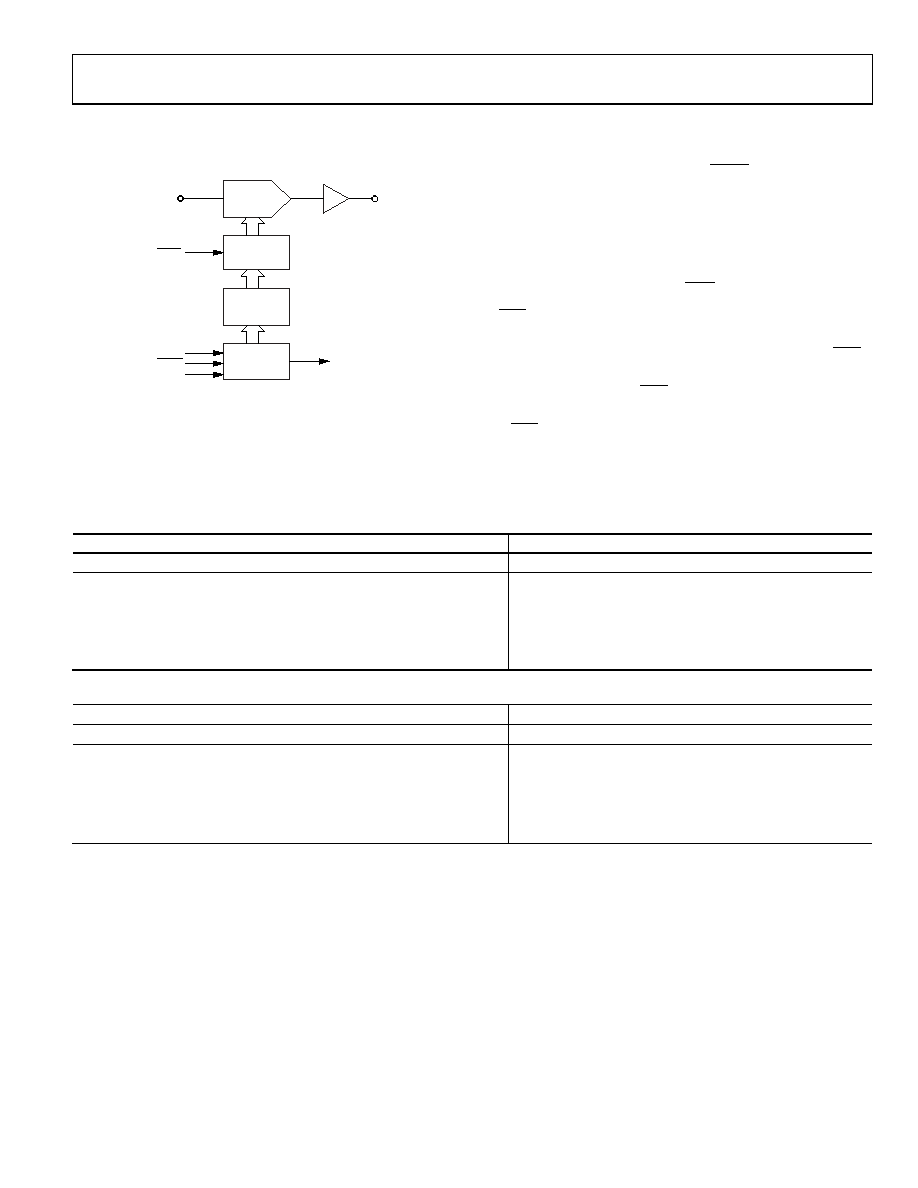
See Figure 41 for a simplified block diagram of the DAC load
circuitry.
VOUTx
DATA
REGISTER
INTERFACE
LOGIC
OUTPUT
I/V AMPLIFIER
LDAC
SDO
SDIN
16-BIT
DAC
REFAB, REFCD
SYNC
INPUT
REGISTER
SCLK
06064-
062
Figure 41. Simplified Serial Interface of Input Loading Circuitry
for One DAC Channel
TRANSFER FUNCTION
Table 7 and Table 8 show the ideal input code to output voltage
relationship for offset binary data coding and twos complement
data coding, respectively.
The output voltage expression for the AD5764R is given by
×
+
×
=
536
,
65
4
2
D
V
REFIN
OUT
where:
D is the decimal equivalent of the code loaded to the DAC.
VREFIN is the reference voltage applied at the REFAB and
REFCD pins.
ASYNCHRONOUS CLEAR (CLR)
CLR is a negative edge triggered clear that allows the outputs to
be cleared to either 0 V (twos complement coding) or negative
full scale (offset binary coding). It is necessary to maintain CLR
low for a minimum amount of time for the operation to complete
(see Figure 2). When the CLR signal is returned high, the output
remains at the cleared value until a new value is programmed.
If CLR is at 0 V at power-on, all DAC outputs are updated with
the clear value. A clear can also be initiated through software by
writing the command of 0x04XXXX.
Table 7. Ideal Output Voltage to Input Code Relationship—Offset Binary Data Coding
Digital Input
Analog Output
MSB
LSB
VOUT
1111
+2 VREFIN × (32,767/32,768)
1000
0000
0001
+2 VREFIN × (1/32,768)
1000
0000
0 V
0111
1111
2 VREFIN × (1/32,768)
0000
2 VREFIN × (32,767/32,768)
Table 8. Ideal Output Voltage to Input Code Relationship—Twos Complement Data Coding
Digital Input
Analog Output
MSB
LSB
VOUT
0111
1111
+2 VREFIN × (32,767/32,768)
0000
0001
+2 VREFIN × (1/32,768)
0000
0 V
1111
2 VREFIN × (1/32,768)
1000
0000
2 VREFIN × (32,767/32,768)
相关PDF资料 |
PDF描述 |
|---|---|
| MS27497E16F26SLC | CONN HSG RCPT 26POS WALL MT SCKT |
| VI-21H-MY-F2 | CONVERTER MOD DC/DC 52V 50W |
| VE-23P-MY-F4 | CONVERTER MOD DC/DC 13.8V 50W |
| VI-21F-MY-F4 | CONVERTER MOD DC/DC 72V 50W |
| MS27505E17B35BC | CONN HSG RCPT 55POS BOX MT SCKT |
相关代理商/技术参数 |
参数描述 |
|---|---|
| AD5764RCSUZ-REEL7 | 功能描述:IC DAC QUAD 16BIT VOUT 32-TQFP RoHS:是 类别:集成电路 (IC) >> 数据采集 - 数模转换器 系列:- 产品培训模块:Lead (SnPb) Finish for COTS Obsolescence Mitigation Program 标准包装:1,000 系列:- 设置时间:1µs 位数:8 数据接口:串行 转换器数目:8 电压电源:双 ± 功率耗散(最大):941mW 工作温度:0°C ~ 70°C 安装类型:表面贴装 封装/外壳:24-SOIC(0.295",7.50mm 宽) 供应商设备封装:24-SOIC W 包装:带卷 (TR) 输出数目和类型:8 电压,单极 采样率(每秒):* |
| AD5764SSUZ-EP-RL7 | 功能描述:16 Bit Digital to Analog Converter 4 32-TQFP (7x7) 制造商:analog devices inc. 系列:iCMOS? 包装:剪切带(CT) 零件状态:有效 位数:16 数模转换器数:4 建立时间:10μs 输出类型:Voltage - Buffered 差分输出:无 数据接口:SPI,DSP 参考类型:外部 电压 - 电源,模拟:±11.4 V ~ 16.5 V 电压 - 电源,数字:2.7 V ~ 5.25 V INL/DNL(LSB):±2(最大),±1(最大) 架构:R-2R 工作温度:-55°C ~ 125°C 封装/外壳:32-TQFP 供应商器件封装:32-TQFP(7x7) 标准包装:1 |
| AD5765 | 制造商:AD 制造商全称:Analog Devices 功能描述:Complete Quad, 16-Bit, High Accuracy, Serial Input, ±5V DACs |
| AD5765BSUZ | 功能描述:IC DAC 16BIT +/-5V QUAD 2LSB 32L RoHS:是 类别:集成电路 (IC) >> 数据采集 - 数模转换器 系列:- 产品培训模块:Data Converter Fundamentals DAC Architectures 标准包装:750 系列:- 设置时间:7µs 位数:16 数据接口:并联 转换器数目:1 电压电源:双 ± 功率耗散(最大):100mW 工作温度:0°C ~ 70°C 安装类型:表面贴装 封装/外壳:28-LCC(J 形引线) 供应商设备封装:28-PLCC(11.51x11.51) 包装:带卷 (TR) 输出数目和类型:1 电压,单极;1 电压,双极 采样率(每秒):143k |
| AD5765BSUZ-REEL7 | 功能描述:IC DAC 16BIT 5V QUAD 32-TQFP RoHS:是 类别:集成电路 (IC) >> 数据采集 - 数模转换器 系列:- 产品培训模块:Data Converter Fundamentals DAC Architectures 标准包装:750 系列:- 设置时间:7µs 位数:16 数据接口:并联 转换器数目:1 电压电源:双 ± 功率耗散(最大):100mW 工作温度:0°C ~ 70°C 安装类型:表面贴装 封装/外壳:28-LCC(J 形引线) 供应商设备封装:28-PLCC(11.51x11.51) 包装:带卷 (TR) 输出数目和类型:1 电压,单极;1 电压,双极 采样率(每秒):143k |
发布紧急采购,3分钟左右您将得到回复。