- 您现在的位置:买卖IC网 > PDF目录10977 > AD5934YRSZ-REEL7 (Analog Devices Inc)IC CONV 12BIT 250KSPS 16SSOP PDF资料下载
参数资料
| 型号: | AD5934YRSZ-REEL7 |
| 厂商: | Analog Devices Inc |
| 文件页数: | 18/32页 |
| 文件大小: | 0K |
| 描述: | IC CONV 12BIT 250KSPS 16SSOP |
| 产品培训模块: | Direct Digital Synthesis Tutorial Series (1 of 7): Introduction Direct Digital Synthesizer Tutorial Series (7 of 7): DDS in Action Direct Digital Synthesis Tutorial Series (3 of 7): Angle to Amplitude Converter Direct Digital Synthesis Tutorial Series (6 of 7): SINC Envelope Correction Direct Digital Synthesis Tutorial Series (4 of 7): Digital-to-Analog Converter Direct Digital Synthesis Tutorial Series (2 of 7): The Accumulator |
| 标准包装: | 500 |
| 分辨率(位): | 12 b |
| 主 fclk: | 16.776MHz |
| 电源电压: | 2.7 V ~ 5.5 V |
| 工作温度: | -40°C ~ 125°C |
| 安装类型: | 表面贴装 |
| 封装/外壳: | 16-SSOP(0.209",5.30mm 宽) |
| 供应商设备封装: | 16-SSOP |
| 包装: | 带卷 (TR) |
| 配用: | EVAL-AD5934EBZ-ND - BOARD EVALUATION FOR AD5934 |
第1页第2页第3页第4页第5页第6页第7页第8页第9页第10页第11页第12页第13页第14页第15页第16页第17页当前第18页第19页第20页第21页第22页第23页第24页第25页第26页第27页第28页第29页第30页第31页第32页
Data Sheet
AD5934
Rev. C | Page 25 of 32
WRITING/READING TO THE AD5934
The I2C interface specification defines several different protocols
for different types of read and write operations. This section
describes the protocols used in the AD5934. The figures in this
section use the abbreviations shown in Table 14.
Table 14. I2C Abbreviation Table
Abbreviation
Condition
S
Start
P
Stop
R
Read
W
Write
A
Acknowledge
A
No acknowledge write byte/command byte
User Command Codes
The command codes in Table 15 are used for reading/writing to
the interface. They are explained in detail in this section but are
grouped within Table 15 for easy reference.
Table 15. Command Codes
Command
Code
Name
Code Description
1010 0000
Block
Write
This command is used when writing
multiple bytes to the RAM; see the
Block Write section.
1010 0001
Block
Read
This command is used when reading
multiple bytes from RAM/memory; see
the Block Read section.
1011 0000
Address
Pointer
This command enables the user to set
the address pointer to any location in
the memory; the data contains the
address of the register to which the
pointer should be pointing.
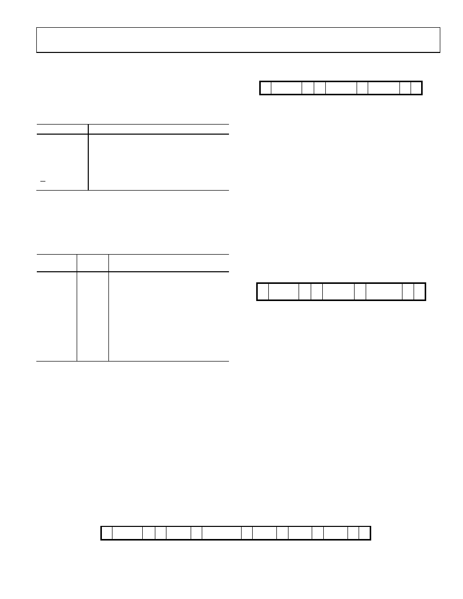
Write Byte/Command Byte
In this operation, the master device sends a byte of data to the
slave device. The write byte can either be a data byte write to a
Register Address or it can be a command operation. To write data
to a register, the command sequence is as follows (see Figure 26):
1. The master device asserts a start condition on SDA.
2. The master sends the 7-bit slave address followed by the
write bit (low).
3. The addressed slave device asserts an acknowledge on SDA.
4. The master sends a register address.
5. The slave asserts an acknowledge on SDA.
6. The master sends a data byte.
7. The slave asserts an acknowledge on SDA.
8. The master asserts a stop condition on SDA to end the
transaction.
S
SLAVE
ADDRESS
REGISTER
ADDRESS
REGISTER
DATA
A
W
A
P
05325-
049
Figure 26. Writing Register Data to Register Address
In the AD5934, the write byte protocol is also used to set a
pointer to a register address (see Figure 27). This protocol is
used for a subsequent single-byte read from the same address,
block read, or block write starting at that address.
To set a register pointer, the following sequence is applied:
1. The master device asserts a start condition on SDA.
2. The master sends the 7-bit slave address followed by the
write bit (low).
3. The addressed slave device asserts an acknowledge on SDA.
4. The master sends a pointer command code (see Table 15, an
address pointer = 1011 0000).
5. The slave asserts an acknowledge on SDA.
6. The master sends a data byte (a register address to where
the pointer is to point).
7. The slave asserts an acknowledge on SDA.
8. The master asserts a stop condition on SDA to end the
transaction.
S
A
W
A
P
POINTER
COMMAND
1011 0000
SLAVE
ADDRESS
REGISTER
ADDRESS
TO POINT TO
05325-
050
Figure 27. Setting Address Pointer to Register Address
BLOCK WRITE
In this operation, the master device writes a block of data to a
slave device (see Figure 28). The start address for a block write
must previously have been set. In the case of the AD5934, this is
done by setting a pointer to set the register address.
1. The master device asserts a start condition on SDA.
2. The master sends the 7-bit slave address followed by the
write bit (low).
3. The addressed slave device asserts an acknowledge on SDA.
4. The master sends an 8-bit command code (1010 0000) that
tells the slave device to expect a block write.
5. The slave asserts an acknowledge on SDA.
6. The master sends a data byte that tells the slave device the
number of data bytes to be sent to it.
7. The slave asserts an acknowledge on SDA.
8. The master sends the data bytes.
9. The slave asserts an acknowledge on SDA after each data byte.
10. The master asserts a stop condition on SDA to end the
transaction.
A
S
W
A
P
SLAVE
ADDRESS
BLOCK
WRITE
NUMBER
BYTES WRITE
BYTE 0
BYTE 1
BYTE 2
05325-
051
Figure 28. Writing a Block Write
相关PDF资料 |
PDF描述 |
|---|---|
| VE-B1D-IX-B1 | CONVERTER MOD DC/DC 85V 75W |
| AD9833BRMZ-REEL7 | IC WAVEFORM GEN PROG 10MSOP |
| VE-B1D-IW-B1 | CONVERTER MOD DC/DC 85V 100W |
| MCF51AC256BCFUE | MCU 32BIT 256K FLASH 64-QFP |
| AD9833BRMZ-REEL | IC WAVEFORM GEN PROG 10MSOP |
相关代理商/技术参数 |
参数描述 |
|---|---|
| AD594 | 制造商:AD 制造商全称:Analog Devices 功能描述:Monolithic Thermocouple Amplifiers with Cold Junction Compensation |
| AD594A | 制造商:AD 制造商全称:Analog Devices 功能描述:Monolithic Thermocouple Amplifiers with Cold Junction Compensation |
| AD594AD | 制造商:Analog Devices 功能描述:Temp Sensor Analog 14-Pin TO-116 制造商:Rochester Electronics LLC 功能描述:THERMOCOUPLER AMPLIFIER - Bulk 制造商:Analog Devices 功能描述:Special Function IC Package/Case:TO-116 |
| AD594AD/+ | 制造商:Rochester Electronics LLC 功能描述:- Bulk |
| AD594ADZ | 功能描述:IC THERMOCOUPLE INSTR AMP 14CDIP RoHS:是 类别:集成电路 (IC) >> PMIC - 热管理 系列:- 标准包装:3,000 系列:- 功能:温度开关 传感器类型:内部 感应温度:85°C 分界点 精确度:±6°C(最小值) 拓扑:ADC(三角积分型),比较器,寄存器库 输出类型:开路漏极 输出警报:是 输出风扇:是 电源电压:2.7 V ~ 5.5 V 工作温度:-55°C ~ 125°C 安装类型:表面贴装 封装/外壳:SC-74A,SOT-753 供应商设备封装:SOT-23-5 包装:带卷 (TR) 其它名称:ADT6501SRJZP085RL7-ND |
发布紧急采购,3分钟左右您将得到回复。