参数资料
| 型号: | AD605AR |
| 厂商: | Analog Devices Inc |
| 文件页数: | 6/25页 |
| 文件大小: | 0K |
| 描述: | IC AMP VGA DUAL LN 40MA 16SOIC |
| 标准包装: | 1 |
| 系列: | X-AMP® |
| 放大器类型: | 可变增益 |
| 电路数: | 2 |
| 转换速率: | 170 V/µs |
| -3db带宽: | 40MHz |
| 电流 - 输入偏压: | 400nA |
| 电流 - 电源: | 18mA |
| 电流 - 输出 / 通道: | 40mA |
| 电压 - 电源,单路/双路(±): | 4.5 V ~ 5.5 V |
| 工作温度: | -40°C ~ 85°C |
| 安装类型: | 表面贴装 |
| 封装/外壳: | 16-SOIC(0.154",3.90mm 宽) |
| 供应商设备封装: | 16-SOIC |
| 包装: | 管件 |
| 配用: | AD605-EVALZ-ND - BOARD EVALUATION FOR AD605 |
AD605
Rev. F | Page 13 of 24
THEORY OF OPERATION
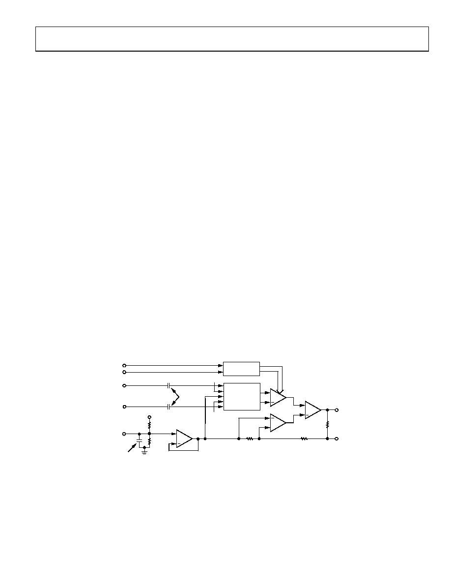
The AD605 is a dual-channel, low noise VGA. Figure 35 shows
the simplified block diagram of one channel. Each channel consists
of a single-supply X-AMP (hereafter called DSX, differential
single-supply X-AMP) comprising the following:
Precision passive attenuator (differential ladder)
Gain control block
VOCM buffer with supply splitting resistors R3 and R4
Active feedback amplifier1 (AFA) with gain setting resistors
R1 and R2
The linear-in-dB gain response of the AD605 can generally be
described by Equation 1.
G (dB) = (Gain Scaling (dB/V)) × (Gain Control (V))
(19 dB (14 dB) × (FB))
(1)
where:
FB = 0, if FBK to OUT is shorted.
FB = 1, if FBK to OUT is open.
Each channel provides between 14 dB to +34.4 dB through
0 dB to +48.4 dB of gain, depending on the value of the resistance
connected between Pin FBK and Pin OUT. The center 40 dB of
gain is exactly linear-in-dB while the gain error increases at the top
and bottom of the range. The gain is set by the gain control voltage
(VGN). The VREF input establishes the gain scaling. The useful
gain scaling range is between 20 dB/V and 40 dB/V for a VREF
voltage of 2.5 V and 1.25 V, respectively. For example, if FBK to
OUT is shorted and VREF is set to 2.50 V (to establish a gain
scaling of 20 dB/V), the gain equation simplifies to
G (dB) = (20 (dB/V)) × (VGN (V)) – 19 dB
(2)
The desired gain can then be achieved by setting the unipolar
gain control (VGN) to a voltage within its nominal operating
range of 0.25 V to 2.65 V (for 20 dB/V gain scaling). The gain is
monotonic for a complete gain control range of 0.1 V to 2.9 V.
Maximum gain can be achieved at a VGN of 2.9 V.
Because the two channels are identical, only Channel 1 is used
to describe their operation. VREF and VOCM are the only inputs
that are shared by the two channels, and because they are normally
ac grounds, crosstalk between the two channels is minimized.
For the highest gain scaling accuracy, VREF should have an
external low impedance voltage source. For low accuracy 20 dB/V
applications, the VREF input can be decoupled with a capacitor
to ground. In this mode, the gain scaling is determined by the
midpoint between +VCC and GND; therefore, care should be
taken to control the supply voltage to 5 V. The input resistance
looking into the VREF pin is 10 kΩ ± 20%.
The AD605 is a single-supply circuit, and the VOCM pin is used
to establish the dc level of the midpoint of this portion of the
circuit. VOCM needs only an external decoupling capacitor to
ground to center the midpoint between the supply voltages (5 V,
GND). However, if the dc level of the output is important to the
user (see the Applications Information section of the AD9050
data sheet for an example), VOCM can be specifically set. The
input resistance looking into the VOCM pin is 45 kΩ ± 20%.
1 To understand the active-feedback amplifier topology, refer to the AD830
data sheet. The AD830 is a practical implementation of the idea.
R1
820
VREF
VGN
VPOS
VOCM
R3
200k
C3
OUT
DISTRIBUTED gm
175
G1
GAIN
CONTROL
Ao
G2
R2
20
R4
200k
EXT
+IN
–IN
FBK
3.36k
DIFFERENTIAL
ATTENUATOR
EXT
C2
C1
00
54
1-
03
6
+
Figure 35. Simplified Block Diagram of a Single Channel of the AD605
相关PDF资料 |
PDF描述 |
|---|---|
| 3314-600T02TC | CONN HEADER 14POS STR NO LATCH |
| 961115-5500-AR-PR | CONN HEADER R/A 15POS GOLD SMD |
| 961117-5500-AR-PT | CONN HEADER R/A 17POS GOLD SMD |
| 3314-52K2 | CONN HEADER 14PS R/A SHORT LATCH |
| 3314-1603 | CONN HEADER 14POS R/A LONG LATCH |
相关代理商/技术参数 |
参数描述 |
|---|---|
| AD605AR-REEL | 功能描述:IC AMP VGA DUAL LN 40MA 16SOIC RoHS:否 类别:集成电路 (IC) >> Linear - Amplifiers - Instrumentation 系列:X-AMP® 标准包装:50 系列:- 放大器类型:J-FET 电路数:2 输出类型:- 转换速率:3.5 V/µs 增益带宽积:1MHz -3db带宽:- 电流 - 输入偏压:30pA 电压 - 输入偏移:2000µV 电流 - 电源:200µA 电流 - 输出 / 通道:- 电压 - 电源,单路/双路(±):7 V ~ 36 V,±3.5 V ~ 18 V 工作温度:0°C ~ 70°C 安装类型:通孔 封装/外壳:8-DIP(0.300",7.62mm) 供应商设备封装:8-PDIP 包装:管件 |
| AD605AR-REEL7 | 功能描述:IC AMP VGA DUAL LN 40MA 16SOIC RoHS:否 类别:集成电路 (IC) >> Linear - Amplifiers - Instrumentation 系列:X-AMP® 标准包装:50 系列:- 放大器类型:J-FET 电路数:2 输出类型:- 转换速率:3.5 V/µs 增益带宽积:1MHz -3db带宽:- 电流 - 输入偏压:30pA 电压 - 输入偏移:2000µV 电流 - 电源:200µA 电流 - 输出 / 通道:- 电压 - 电源,单路/双路(±):7 V ~ 36 V,±3.5 V ~ 18 V 工作温度:0°C ~ 70°C 安装类型:通孔 封装/外壳:8-DIP(0.300",7.62mm) 供应商设备封装:8-PDIP 包装:管件 |
| AD605ARZ | 功能描述:IC AMP VGA DUAL LN 40MA 16SOIC RoHS:是 类别:集成电路 (IC) >> Linear - Amplifiers - Instrumentation 系列:X-AMP® 标准包装:2,500 系列:- 放大器类型:通用 电路数:4 输出类型:- 转换速率:0.6 V/µs 增益带宽积:1MHz -3db带宽:- 电流 - 输入偏压:45nA 电压 - 输入偏移:2000µV 电流 - 电源:1.4mA 电流 - 输出 / 通道:40mA 电压 - 电源,单路/双路(±):3 V ~ 32 V,±1.5 V ~ 16 V 工作温度:0°C ~ 70°C 安装类型:表面贴装 封装/外壳:14-TSSOP(0.173",4.40mm 宽) 供应商设备封装:14-TSSOP 包装:带卷 (TR) 其它名称:LM324ADTBR2G-NDLM324ADTBR2GOSTR |
| AD605ARZ-R7 | 功能描述:IC AMP VGA DUAL LN 40MA 16SOIC RoHS:是 类别:集成电路 (IC) >> Linear - Amplifiers - Instrumentation 系列:X-AMP® 标准包装:50 系列:- 放大器类型:J-FET 电路数:2 输出类型:- 转换速率:3.5 V/µs 增益带宽积:1MHz -3db带宽:- 电流 - 输入偏压:30pA 电压 - 输入偏移:2000µV 电流 - 电源:200µA 电流 - 输出 / 通道:- 电压 - 电源,单路/双路(±):7 V ~ 36 V,±3.5 V ~ 18 V 工作温度:0°C ~ 70°C 安装类型:通孔 封装/外壳:8-DIP(0.300",7.62mm) 供应商设备封装:8-PDIP 包装:管件 |
| AD605ARZ-RL | 功能描述:IC AMP VGA DUAL LN 40MA 16SOIC RoHS:是 类别:集成电路 (IC) >> Linear - Amplifiers - Instrumentation 系列:X-AMP® 标准包装:50 系列:- 放大器类型:J-FET 电路数:2 输出类型:- 转换速率:3.5 V/µs 增益带宽积:1MHz -3db带宽:- 电流 - 输入偏压:30pA 电压 - 输入偏移:2000µV 电流 - 电源:200µA 电流 - 输出 / 通道:- 电压 - 电源,单路/双路(±):7 V ~ 36 V,±3.5 V ~ 18 V 工作温度:0°C ~ 70°C 安装类型:通孔 封装/外壳:8-DIP(0.300",7.62mm) 供应商设备封装:8-PDIP 包装:管件 |
发布紧急采购,3分钟左右您将得到回复。