参数资料
| 型号: | AD605AR |
| 厂商: | Analog Devices Inc |
| 文件页数: | 9/25页 |
| 文件大小: | 0K |
| 描述: | IC AMP VGA DUAL LN 40MA 16SOIC |
| 标准包装: | 1 |
| 系列: | X-AMP® |
| 放大器类型: | 可变增益 |
| 电路数: | 2 |
| 转换速率: | 170 V/µs |
| -3db带宽: | 40MHz |
| 电流 - 输入偏压: | 400nA |
| 电流 - 电源: | 18mA |
| 电流 - 输出 / 通道: | 40mA |
| 电压 - 电源,单路/双路(±): | 4.5 V ~ 5.5 V |
| 工作温度: | -40°C ~ 85°C |
| 安装类型: | 表面贴装 |
| 封装/外壳: | 16-SOIC(0.154",3.90mm 宽) |
| 供应商设备封装: | 16-SOIC |
| 包装: | 管件 |
| 配用: | AD605-EVALZ-ND - BOARD EVALUATION FOR AD605 |
AD605
Rev. F | Page 16 of 24
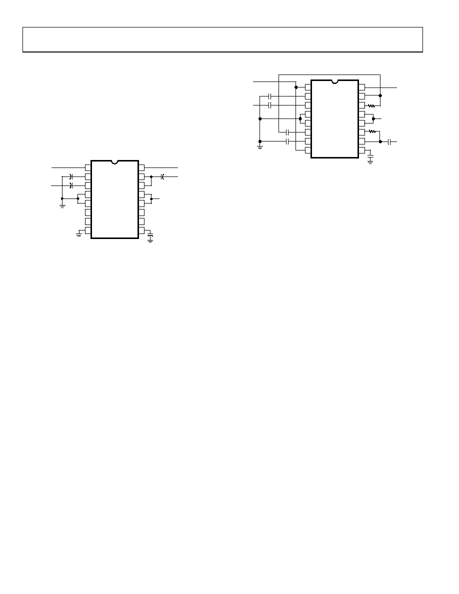
APPLICATIONS INFORMATION
The basic circuit in Figure 38 shows the connections for one
channel of the AD605 with a gain range of 14 dB to +34.4 dB.
The signal is applied at +IN1. The ac coupling capacitors before
Pin IN1 and Pin +IN1 should be selected according to the
required lower cutoff frequency. In this example, the 0.1 μF
capacitors, together with the 175 Ω of each of the DSX input
pins, provide a 3 dB high-pass corner of about 9.1 kHz. The
upper cutoff frequency is determined by the amplifier and is
40 MHz.
14
13
12
11
16
15
10
9
8
1
2
3
4
7
6
5
VREF
GND1
+IN1
–IN1
VGN1
OUT1
FBK1
VPOS
–IN2
+IN2
GND2
VPOS
FBK2
OUT2
VOCM
VGN2
AD605
VGN
VIN
0.1F
5V
0.1F
OUT
2.500V
0
05
41
-03
9
Figure 38. Basic Connections for a Single Channel
As shown in Figure 38, the output is ac-coupled for optimum
performance. In the case of connecting to the 10-bit, 40 MSPS
ADC, AD9050, ac coupling can be eliminated as long as
Pin VOCM is biased by the same 3.3 V common-mode voltage
as the AD9050.
Pin VREF requires a voltage of 1.25 V to 2.5 V, with gain scaling
between 40 dB/V and 20 dB/V, respectively. Voltage VGN controls
the gain; its nominal operating range is from 0.25 V to 2.65 V
for 20 dB/V gain scaling and 0.125 V to 1.325 V for 40 dB/V
scaling. When this pin is taken to ground, the channel powers
down and disables its output.
CONNECTING TWO AMPLIFIERS TO DOUBLE THE
GAIN RANGE
Figure 39 shows the two channels of the AD605 connected in
series to provide a total gain range of 96.8 dB. When R1 and R2
are shorts, the gain range is from 28 dB to +68.8 dB with a
slightly reduced bandwidth of about 30 MHz. The reduction in
bandwidth is due to two identical low-pass circuits being connected
in series; in the case of two identical single-pole, low-pass filters,
the bandwidth is reduced by exactly √2. If R1 and R2 are
replaced by open circuits, that is, Pin FBK1 and Pin FBK2 are left
unconnected, the gain range shifts up by 28 dB to 0 dB to 96.8 dB.
As previously noted, the bandwidth of each individual channel is
reduced by a factor of 5 to about 8 MHz because the gain increased
by 14 dB. In addition, there is still the √2 reduction because the
series connection of the two channels results in a final
bandwidth of the higher gain version of about 6 MHz.
14
13
12
11
16
15
10
9
8
1
2
3
4
7
6
5
VREF
GND1
+IN1
–IN1
VGN1
OUT1
FBK1
VPOS
–IN2
+IN2
GND2
VPOS
FBK2
OUT2
VOCM
VGN2
AD605
C2
0.1F
VGN
VIN
R1
5V
OUT
2.500V
C1
0.1F
C3
0.1F
C4
0.1F
C6
0.1F
R2
C5
0.1F
00
54
1-
0
40
Figure 39. Doubling the Gain Range with Two Amplifiers
Two other easy combinations are possible to provide a gain
range of 14 dB to +82.8 dB: make R1 a short and R2 an open,
or make R1 an open and R2 a short. The bandwidth for both of
these cases is dominated by the channel that is set to the higher
gain and is about 8 MHz. From a noise standpoint, the second
choice is the best because by increasing the gain of the first
amplifier, the noise of the second amplifier has less of an impact
on the total output noise. One further observation regarding
noise is that by increasing the gain, the output noise increases
proportionally; therefore, there is no increase in signal-to-noise
ratio. It actually stays fixed.
It should be noted that by selecting the appropriate values of R1
and R2, any gain range between 28 dB to +68.8 dB and 0 dB to
+96.8 dB can be achieved with the circuit in Figure 39. When
using any value other than shorts and opens for R1 and R2, the
final value of the gain range depends on the external resistors
matching the on-chip resistors. Because the internal resistors
can vary by as much as ±20%, the actual values for a particular
gain have to be determined empirically. Note that the two channels
within one part match quite well; therefore, R1 tracks R2 in
C3 is not required because the common-mode voltage at
Pin OUT1 should be identical to the one at Pin +IN2 and
Pin IN2. However, because only 1 mV of offset at the output
of the first DSX introduces an offset of 53 mV when the second
DSX is set to the maximum gain of the lowest gain range (34.4 dB),
and 263 mV when set to the maximum gain of the highest gain
range (48.4 dB), it is important to include ac coupling to get the
maximum dynamic range at the output of the cascaded amplifiers.
C5 is necessary if the output signal needs to be referenced to any
common-mode level other than half of the supply as is provided
by Pin OUT2.
相关PDF资料 |
PDF描述 |
|---|---|
| 3314-600T02TC | CONN HEADER 14POS STR NO LATCH |
| 961115-5500-AR-PR | CONN HEADER R/A 15POS GOLD SMD |
| 961117-5500-AR-PT | CONN HEADER R/A 17POS GOLD SMD |
| 3314-52K2 | CONN HEADER 14PS R/A SHORT LATCH |
| 3314-1603 | CONN HEADER 14POS R/A LONG LATCH |
相关代理商/技术参数 |
参数描述 |
|---|---|
| AD605AR-REEL | 功能描述:IC AMP VGA DUAL LN 40MA 16SOIC RoHS:否 类别:集成电路 (IC) >> Linear - Amplifiers - Instrumentation 系列:X-AMP® 标准包装:50 系列:- 放大器类型:J-FET 电路数:2 输出类型:- 转换速率:3.5 V/µs 增益带宽积:1MHz -3db带宽:- 电流 - 输入偏压:30pA 电压 - 输入偏移:2000µV 电流 - 电源:200µA 电流 - 输出 / 通道:- 电压 - 电源,单路/双路(±):7 V ~ 36 V,±3.5 V ~ 18 V 工作温度:0°C ~ 70°C 安装类型:通孔 封装/外壳:8-DIP(0.300",7.62mm) 供应商设备封装:8-PDIP 包装:管件 |
| AD605AR-REEL7 | 功能描述:IC AMP VGA DUAL LN 40MA 16SOIC RoHS:否 类别:集成电路 (IC) >> Linear - Amplifiers - Instrumentation 系列:X-AMP® 标准包装:50 系列:- 放大器类型:J-FET 电路数:2 输出类型:- 转换速率:3.5 V/µs 增益带宽积:1MHz -3db带宽:- 电流 - 输入偏压:30pA 电压 - 输入偏移:2000µV 电流 - 电源:200µA 电流 - 输出 / 通道:- 电压 - 电源,单路/双路(±):7 V ~ 36 V,±3.5 V ~ 18 V 工作温度:0°C ~ 70°C 安装类型:通孔 封装/外壳:8-DIP(0.300",7.62mm) 供应商设备封装:8-PDIP 包装:管件 |
| AD605ARZ | 功能描述:IC AMP VGA DUAL LN 40MA 16SOIC RoHS:是 类别:集成电路 (IC) >> Linear - Amplifiers - Instrumentation 系列:X-AMP® 标准包装:2,500 系列:- 放大器类型:通用 电路数:4 输出类型:- 转换速率:0.6 V/µs 增益带宽积:1MHz -3db带宽:- 电流 - 输入偏压:45nA 电压 - 输入偏移:2000µV 电流 - 电源:1.4mA 电流 - 输出 / 通道:40mA 电压 - 电源,单路/双路(±):3 V ~ 32 V,±1.5 V ~ 16 V 工作温度:0°C ~ 70°C 安装类型:表面贴装 封装/外壳:14-TSSOP(0.173",4.40mm 宽) 供应商设备封装:14-TSSOP 包装:带卷 (TR) 其它名称:LM324ADTBR2G-NDLM324ADTBR2GOSTR |
| AD605ARZ-R7 | 功能描述:IC AMP VGA DUAL LN 40MA 16SOIC RoHS:是 类别:集成电路 (IC) >> Linear - Amplifiers - Instrumentation 系列:X-AMP® 标准包装:50 系列:- 放大器类型:J-FET 电路数:2 输出类型:- 转换速率:3.5 V/µs 增益带宽积:1MHz -3db带宽:- 电流 - 输入偏压:30pA 电压 - 输入偏移:2000µV 电流 - 电源:200µA 电流 - 输出 / 通道:- 电压 - 电源,单路/双路(±):7 V ~ 36 V,±3.5 V ~ 18 V 工作温度:0°C ~ 70°C 安装类型:通孔 封装/外壳:8-DIP(0.300",7.62mm) 供应商设备封装:8-PDIP 包装:管件 |
| AD605ARZ-RL | 功能描述:IC AMP VGA DUAL LN 40MA 16SOIC RoHS:是 类别:集成电路 (IC) >> Linear - Amplifiers - Instrumentation 系列:X-AMP® 标准包装:50 系列:- 放大器类型:J-FET 电路数:2 输出类型:- 转换速率:3.5 V/µs 增益带宽积:1MHz -3db带宽:- 电流 - 输入偏压:30pA 电压 - 输入偏移:2000µV 电流 - 电源:200µA 电流 - 输出 / 通道:- 电压 - 电源,单路/双路(±):7 V ~ 36 V,±3.5 V ~ 18 V 工作温度:0°C ~ 70°C 安装类型:通孔 封装/外壳:8-DIP(0.300",7.62mm) 供应商设备封装:8-PDIP 包装:管件 |
发布紧急采购,3分钟左右您将得到回复。