参数资料
| 型号: | AD605AR |
| 厂商: | Analog Devices Inc |
| 文件页数: | 8/25页 |
| 文件大小: | 0K |
| 描述: | IC AMP VGA DUAL LN 40MA 16SOIC |
| 标准包装: | 1 |
| 系列: | X-AMP® |
| 放大器类型: | 可变增益 |
| 电路数: | 2 |
| 转换速率: | 170 V/µs |
| -3db带宽: | 40MHz |
| 电流 - 输入偏压: | 400nA |
| 电流 - 电源: | 18mA |
| 电流 - 输出 / 通道: | 40mA |
| 电压 - 电源,单路/双路(±): | 4.5 V ~ 5.5 V |
| 工作温度: | -40°C ~ 85°C |
| 安装类型: | 表面贴装 |
| 封装/外壳: | 16-SOIC(0.154",3.90mm 宽) |
| 供应商设备封装: | 16-SOIC |
| 包装: | 管件 |
| 配用: | AD605-EVALZ-ND - BOARD EVALUATION FOR AD605 |
AD605
Rev. F | Page 15 of 24
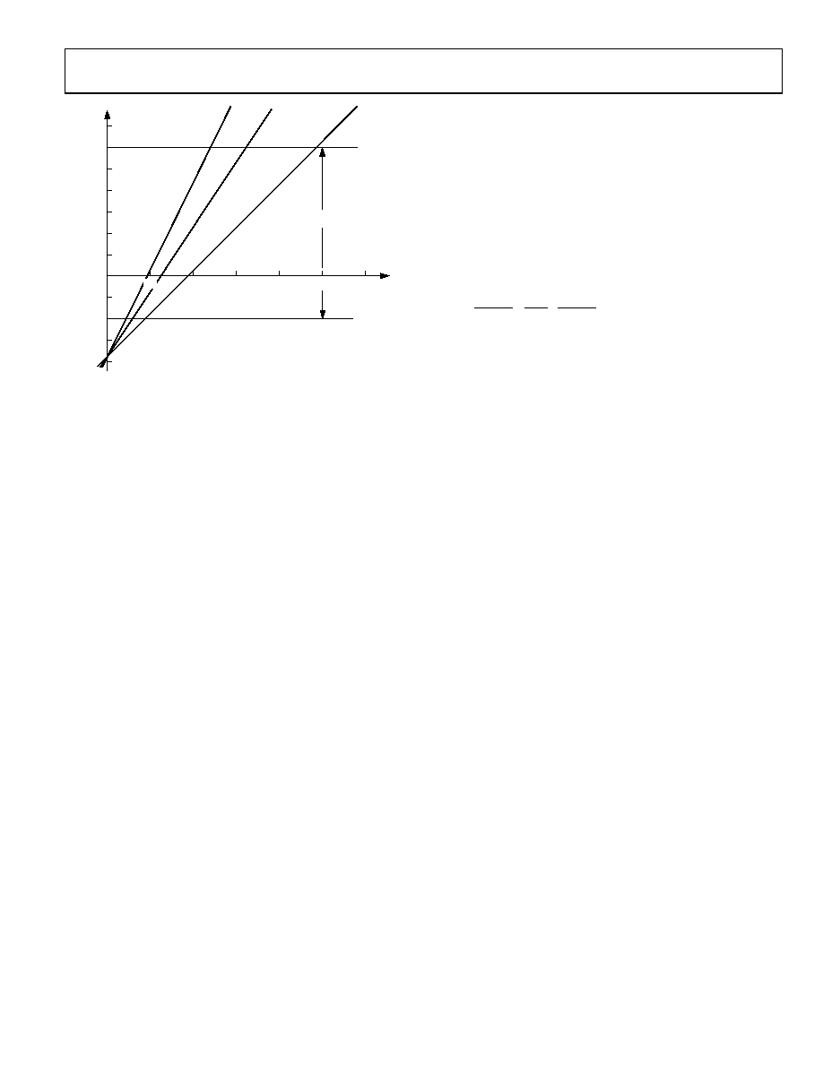
35
30
25
20
15
10
5
0
–5
–10
–15
–20
G
A
IN
(
d
B
)
40dB/V
30dB/V
20dB/V
LINEAR-IN-dB RANGE
OF AD605
1.0
0.5
1.5
2.0
2.5
3.0
GAIN CONTROL VOLTAGE
0
05
41
-03
8
Figure 37. Ideal Gain Curves vs. VREF
Usable gain control voltage ranges are 0.1 V to 2.9 V for the
20 dB/V scale and 0.1 V to 1.45 V for the 40 dB/V scale. VGN
voltages of less than 0.1 V are not used for gain control because
below 50 mV the channel is powered down. This can be used to
conserve power and at the same time gate-off the signal. The
supply current for a powered-down channel is 1.9 mA, and the
response time to power the device on or off is less than 1 μs.
FIXED GAIN AMPLIFIER AND INTERPOLATOR
CIRCUITS—APPLYING AN ACTIVE FEEDBACK
AMPLIFIER
A typical X-amp architecture is powered by a dual polarity
power supply. Because the AD605 operates from a single supply, a
supply common equal to half the value of the supply voltage is
required. An active feedback amplifier (AFA) is used to provide
a differential input and to implement the feedback loop. The
AFA in the AD605 is an op amp with two gm stages; one is used
in the feedback path, and the other is used as a highly linear
differential input.
A multisection distributed gm stage senses the voltages on the
ladder network, one stage for each of the ladder nodes. Only a
few of the stages are active at any time and are dependent on the
gain control voltage.
The AFA makes a differential input structure possible because
one of its inputs (G1) is fully differential; this input is made
up of a distributed gm stage. The second input (G2) is used for
feedback. The output of G1 is some function of the voltages
sensed on the attenuator taps that is applied to a high gain
amplifier (A0). Because of negative feedback, the differential
input to the high gain amplifier is zero; this in turn implies that
the differential input voltage to G2 times gm2 (the transconductance
of G2) is equal to the differential input voltage to G1 times gm1
(the transconductance of G1). Therefore, the overall gain
function of the AFA is
R2
R1
g
V
m
ATTEN
OUT
×
=
2
1
(7)
where:
VOUT is the output voltage.
VATTEN is the effective voltage sensed on the attenuator.
(
R1 + R2)/R2 = 42.
gm1/gm2 = 1.25; the overall gain is therefore 52.5 (34.4 dB).
The AFA has additional features that include the following:
inverting the output signal by switching the positive and negative
input to the ladder network; the possibility of using the IN
input as a second signal input; and independent control of the
DSX common-mode voltage. Under normal operating conditions,
it is best to connect a decoupling capacitor to Pin VOCM, in
which case, the common- mode voltage of the DSX is half of
the supply voltage; this allows for maximum signal swing.
Nevertheless, the common-mode voltage can be shifted up or
down by directly applying a voltage to VOCM. It can also be
used as another signal input, the only limitation being the
rather low slew rate of the VOCM buffer.
If the dc level of the output signal is not critical, another coupling
capacitor is normally used at the output of the DSX; again, this
is done for level shifting and to eliminate any dc offsets contributed
by the DSX (see the AC Coupling section).
The gain range of the DSX is programmable by a resistor connected
between Pin FBK and Pin OUT. The possible ranges are 14 dB to
+34.4 dB when the pins are shorted together or 0 dB to +48.4 dB
when FBK is left open. For the higher gain range, the bandwidth
of the amplifier is reduced by a factor of five to about 8 MHz
because the gain increased by 14 dB. This is the case for any
constant gain bandwidth product amplifier that includes the
active feedback amplifier.
相关PDF资料 |
PDF描述 |
|---|---|
| 3314-600T02TC | CONN HEADER 14POS STR NO LATCH |
| 961115-5500-AR-PR | CONN HEADER R/A 15POS GOLD SMD |
| 961117-5500-AR-PT | CONN HEADER R/A 17POS GOLD SMD |
| 3314-52K2 | CONN HEADER 14PS R/A SHORT LATCH |
| 3314-1603 | CONN HEADER 14POS R/A LONG LATCH |
相关代理商/技术参数 |
参数描述 |
|---|---|
| AD605AR-REEL | 功能描述:IC AMP VGA DUAL LN 40MA 16SOIC RoHS:否 类别:集成电路 (IC) >> Linear - Amplifiers - Instrumentation 系列:X-AMP® 标准包装:50 系列:- 放大器类型:J-FET 电路数:2 输出类型:- 转换速率:3.5 V/µs 增益带宽积:1MHz -3db带宽:- 电流 - 输入偏压:30pA 电压 - 输入偏移:2000µV 电流 - 电源:200µA 电流 - 输出 / 通道:- 电压 - 电源,单路/双路(±):7 V ~ 36 V,±3.5 V ~ 18 V 工作温度:0°C ~ 70°C 安装类型:通孔 封装/外壳:8-DIP(0.300",7.62mm) 供应商设备封装:8-PDIP 包装:管件 |
| AD605AR-REEL7 | 功能描述:IC AMP VGA DUAL LN 40MA 16SOIC RoHS:否 类别:集成电路 (IC) >> Linear - Amplifiers - Instrumentation 系列:X-AMP® 标准包装:50 系列:- 放大器类型:J-FET 电路数:2 输出类型:- 转换速率:3.5 V/µs 增益带宽积:1MHz -3db带宽:- 电流 - 输入偏压:30pA 电压 - 输入偏移:2000µV 电流 - 电源:200µA 电流 - 输出 / 通道:- 电压 - 电源,单路/双路(±):7 V ~ 36 V,±3.5 V ~ 18 V 工作温度:0°C ~ 70°C 安装类型:通孔 封装/外壳:8-DIP(0.300",7.62mm) 供应商设备封装:8-PDIP 包装:管件 |
| AD605ARZ | 功能描述:IC AMP VGA DUAL LN 40MA 16SOIC RoHS:是 类别:集成电路 (IC) >> Linear - Amplifiers - Instrumentation 系列:X-AMP® 标准包装:2,500 系列:- 放大器类型:通用 电路数:4 输出类型:- 转换速率:0.6 V/µs 增益带宽积:1MHz -3db带宽:- 电流 - 输入偏压:45nA 电压 - 输入偏移:2000µV 电流 - 电源:1.4mA 电流 - 输出 / 通道:40mA 电压 - 电源,单路/双路(±):3 V ~ 32 V,±1.5 V ~ 16 V 工作温度:0°C ~ 70°C 安装类型:表面贴装 封装/外壳:14-TSSOP(0.173",4.40mm 宽) 供应商设备封装:14-TSSOP 包装:带卷 (TR) 其它名称:LM324ADTBR2G-NDLM324ADTBR2GOSTR |
| AD605ARZ-R7 | 功能描述:IC AMP VGA DUAL LN 40MA 16SOIC RoHS:是 类别:集成电路 (IC) >> Linear - Amplifiers - Instrumentation 系列:X-AMP® 标准包装:50 系列:- 放大器类型:J-FET 电路数:2 输出类型:- 转换速率:3.5 V/µs 增益带宽积:1MHz -3db带宽:- 电流 - 输入偏压:30pA 电压 - 输入偏移:2000µV 电流 - 电源:200µA 电流 - 输出 / 通道:- 电压 - 电源,单路/双路(±):7 V ~ 36 V,±3.5 V ~ 18 V 工作温度:0°C ~ 70°C 安装类型:通孔 封装/外壳:8-DIP(0.300",7.62mm) 供应商设备封装:8-PDIP 包装:管件 |
| AD605ARZ-RL | 功能描述:IC AMP VGA DUAL LN 40MA 16SOIC RoHS:是 类别:集成电路 (IC) >> Linear - Amplifiers - Instrumentation 系列:X-AMP® 标准包装:50 系列:- 放大器类型:J-FET 电路数:2 输出类型:- 转换速率:3.5 V/µs 增益带宽积:1MHz -3db带宽:- 电流 - 输入偏压:30pA 电压 - 输入偏移:2000µV 电流 - 电源:200µA 电流 - 输出 / 通道:- 电压 - 电源,单路/双路(±):7 V ~ 36 V,±3.5 V ~ 18 V 工作温度:0°C ~ 70°C 安装类型:通孔 封装/外壳:8-DIP(0.300",7.62mm) 供应商设备封装:8-PDIP 包装:管件 |
发布紧急采购,3分钟左右您将得到回复。