参数资料
| 型号: | AD606JN |
| 厂商: | Analog Devices Inc |
| 文件页数: | 9/12页 |
| 文件大小: | 0K |
| 描述: | IC AMP LOG LP 1.2MA 16DIP |
| 标准包装: | 1 |
| 放大器类型: | 对数 |
| 电路数: | 1 |
| 输出类型: | 差分 |
| 电流 - 输入偏压: | 4µA |
| 电流 - 电源: | 13mA |
| 电流 - 输出 / 通道: | 1.2mA |
| 电压 - 电源,单路/双路(±): | 4.5 V ~ 5.5 V |
| 工作温度: | 0°C ~ 70°C |
| 安装类型: | 通孔 |
| 封装/外壳: | 16-DIP(0.300",7.62mm) |
| 供应商设备封装: | 16-PDIP |
| 包装: | 管件 |
AD606
REV. B
–6–
Offset-Control Loop
The offset-control loop nulls the input offset voltage, and sets
up the bias voltages at the input pins INHI and INLO. A full
understanding of this offset-control loop is useful, particularly
when using larger input coupling capacitors and an external
filter capacitor to lower the minimum acceptable operating
frequency. The loop’s primary purpose is to extend the lower
end of the dynamic range in the case where the offset voltage of
the first stage should be high enough to cause later stages to
prematurely enter limiting, because of the high dc gain (about
8000) of the main amplifier system. For example, an offset
voltage of only 20
V would become 160 mV at the output of
the last stage in the main amplifier (before the final limiter sec-
tion), driving the last stage well into limiting. In the absence of
noise, this limiting would simply result in the logarithmic output
ceasing to become any lower below a certain signal level at the
input. The offset would also degrade the logarithmic conform-
ance in this region. In practice, the finite noise of the first stage
also plays a role in this regard, even if the dc offset were zero.
Figure 3 shows a representation of this loop, reduced to essen-
tials. The figure closely corresponds to the internal circuitry,
and correctly shows the input resistance. Thus, the forward gain
of the main amplifier section is 7
× 11.15 dB, but the loop gain
is lowered because of the attenuation in the network formed by
RB1 and RB2 and the input resistance RA. The connection
polarity is such as to result in negative feedback, which reduces
the input offset voltage by the dc loop gain, here about 50 dB,
that is, by a factor of about 316. We use a differential representa-
tion, because later we will examine the consequences to the
power-up response time in the event that the ac coupling capaci-
tors CC1 and CC2 do not exactly match. Note that these capaci-
tors, as well as forming a high-pass filter to the signal in the
forward path, also introduce a pole in the feedback path.
TO FINAL
LIMITER
STAGE
+1
RB1
30k
RB2
30k
RA
2.5k
CF2
30pF
CF1
30pF
0V
RF2
360k
RF1
360k
FIL2
FIL1
CZ
RZ
CC1
CC2
78dB
Figure 3. Offset Control Loop
Internal resistors RF1 and RF2 in conjunction with grounded
capacitors CF1 and CF2 form a low-pass filter at 15 kHz. This
frequency can optionally be lowered by the addition of an exter-
nal capacitor CZ, and in some cases a series resistor RZ. This, in
conjunction with the low-pass section formed at the input cou-
pling, results in a two-pole high-pass response, falling of at
40 dB/decade below the corner frequency. The damping factor
of this filter depends on the ratio CZ/CC (when CZ>>CF) and
also on the value of RZ.
The inclusion of this control loop has no effect on the high frequency
response of the AD606. Nor does it have any effect on the low fre-
quency response when the input amplitude is substantially above the
input offset voltage.
The loop’s effect is felt only at the lower end of the dynamic
range, that is, from about 80 dBm to –70 dBm, and when the
signal frequency is near the lower edge of the passband. Thus,
the small signal results which are obtained using the suggested
model are not indicative of the ac response at moderate to high
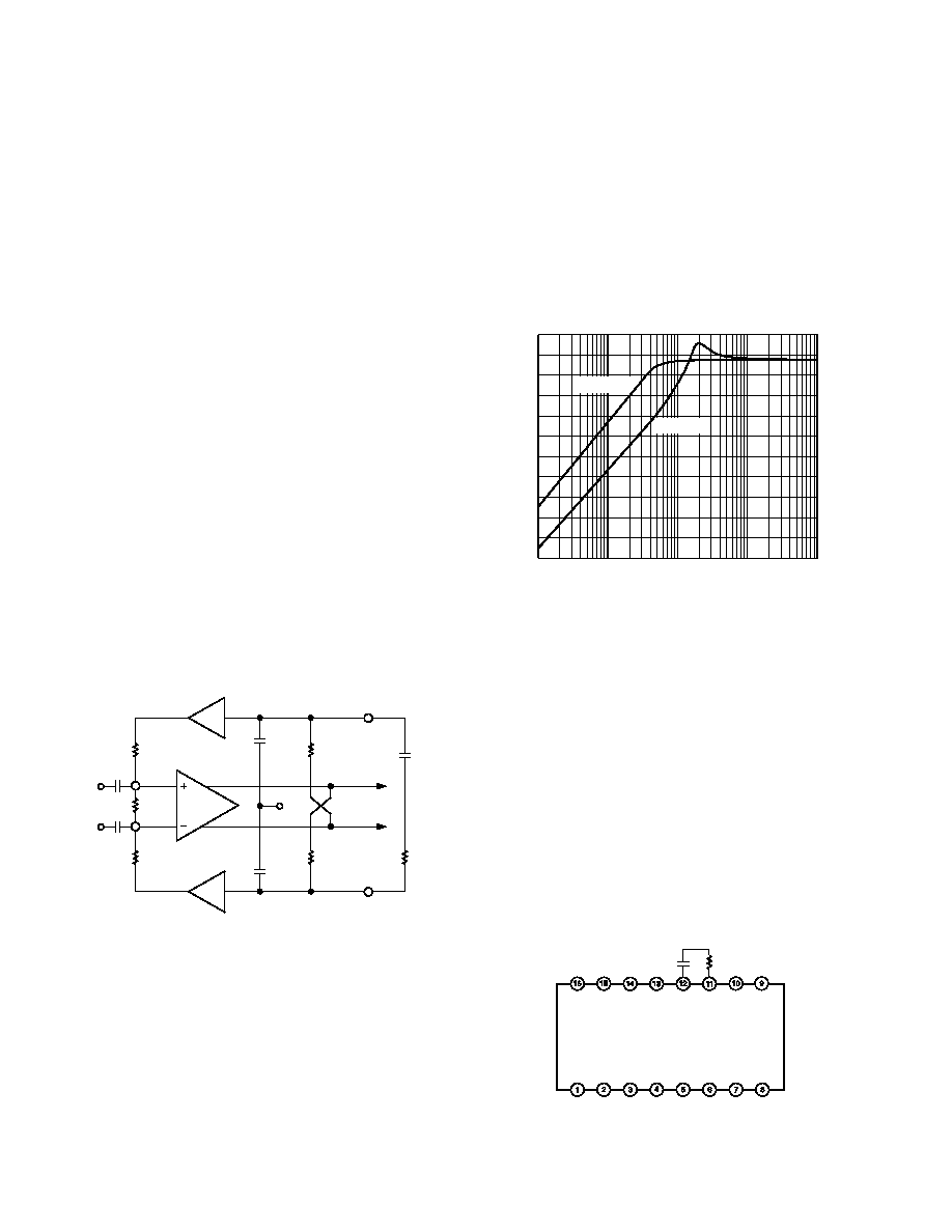
signal levels. Figure 4 shows the response of this model for the
default case (using CC = 100 pF and CZ = 0) and with CZ =
150 pF. In general, a maximally flat ac response occurs when CZ
is roughly twice CC (making due allowance for the internal
30 pF capacitors). Thus, for audio applications, one can use
CC = 2.7 F and CZ = 4.7 F to achieve a high-pass corner
(–3 dB) at 25 Hz.
90
70
–20
100k
100M
10M
1M
10k
80
60
40
50
20
30
10
–10
0
INPUT FREQUENCY – Hz
RELATIVE
OUTPUT
–
dB
CZ = 150pF
CZ = 0pF
Figure 4. Frequency Response of Offset Control Loop for
CZ = 0 pF and CZ = 150 pF (CC = 100 pF)
However, the maximally flat ac response is not optimal in two
special cases. First, where the RF input level is rapidly pulsed,
the fast edges will cause the loop filter to ring. Second, ringing
can also occur when using the power-up feature, and the ac
coupling capacitors do not exactly match in value. We will ex-
amine the latter case in a moment. Ringing in a linear amplifier
is annoying, but in a log amp, with its much enhanced sensitiv-
ity to near zero signals, it can be very disruptive.
To optimize the low level accuracy, that is, achieve a highly
damped pulse response in this filter, it is recommended to in-
clude a resistor RZ in series with an increased value of CZ. Some
experimentation may be necessary, but for operation in the
range 3 MHz to 70 MHz, values of CC = 100 pF, CZ = 1 nF
and RZ = 2 k are near optimal. For operation down to 100 kHz
use CC = 10 nF, CZ = 0.1 F and RZ = 13 k. Figure 5 shows
typical connections for the AD606 with these filter components
added.
INHI
COMM
PRUP
VPOS
FIL1
FIL2
LADJ
LMHI
INLO
COMM
ISUM
ILOG
BFIN
VLOG
OPCM
LMLO
AD606JN
RZ
CZ
Figure 5. Use of CZ and RZ for Offset Control Loop
Compensation
相关PDF资料 |
PDF描述 |
|---|---|
| TV02W101B-HF | TVS 200W 100V BIDIRECT SOD-123 |
| TV02W101B-G | TVS 200W 100V BIDIRECT SOD-123 |
| TLC2272CPSRG4 | IC OPAMP GP R-R 2.25MHZ 8SOIC |
| TV02W100B-HF | TVS 200W 10V BIDIRECT SOD-123 |
| 86584-214HLF | BERGSTIK II DR STRAIGHT RET |
相关代理商/技术参数 |
参数描述 |
|---|---|
| AD606JNZ | 功能描述:IC AMP LOG LP 1.2MA 16DIP RoHS:是 类别:集成电路 (IC) >> Linear - Amplifiers - Instrumentation 系列:- 标准包装:1 系列:- 放大器类型:通用 电路数:4 输出类型:满摆幅 转换速率:0.028 V/µs 增益带宽积:105kHz -3db带宽:- 电流 - 输入偏压:3nA 电压 - 输入偏移:100µV 电流 - 电源:3.3µA 电流 - 输出 / 通道:12mA 电压 - 电源,单路/双路(±):2.7 V ~ 12 V,±1.35 V ~ 6 V 工作温度:-40°C ~ 85°C 安装类型:表面贴装 封装/外壳:14-TSSOP(0.173",4.40mm 宽) 供应商设备封装:14-TSSOP 包装:剪切带 (CT) 其它名称:OP481GRUZ-REELCT |
| AD606JNZ | 制造商:Analog Devices 功能描述:IC AMP ((NS)) |
| AD606JR | 功能描述:IC AMP LOG LP 1.2MA 16SOIC RoHS:否 类别:集成电路 (IC) >> Linear - Amplifiers - Instrumentation 系列:- 其它有关文件:TS1854A View All Specifications 标准包装:50 系列:- 放大器类型:通用 电路数:4 输出类型:满摆幅 转换速率:0.25 V/µs 增益带宽积:630kHz -3db带宽:- 电流 - 输入偏压:16nA 电压 - 输入偏移:1000µV 电流 - 电源:162µA 电流 - 输出 / 通道:48mA 电压 - 电源,单路/双路(±):1.8 V ~ 6 V 工作温度:-40°C ~ 125°C 安装类型:表面贴装 封装/外壳:14-SOIC(0.154",3.90mm 宽) 供应商设备封装:14-SO 包装:管件 |
| AD606JR-REEL | 制造商:Analog Devices 功能描述:SP Amp LOG Amp Single 5.5V 16-Pin SOIC N T/R 制造商:Analog Devices 功能描述:SP AMP LOG AMP SGL 5.5V 16SOIC N - Tape and Reel |
| AD606JR-REEL7 | 功能描述:IC AMP LOG LP 1.2MA 16SOIC RoHS:否 类别:集成电路 (IC) >> Linear - Amplifiers - Instrumentation 系列:- 标准包装:50 系列:- 放大器类型:J-FET 电路数:2 输出类型:- 转换速率:3.5 V/µs 增益带宽积:1MHz -3db带宽:- 电流 - 输入偏压:30pA 电压 - 输入偏移:2000µV 电流 - 电源:200µA 电流 - 输出 / 通道:- 电压 - 电源,单路/双路(±):7 V ~ 36 V,±3.5 V ~ 18 V 工作温度:0°C ~ 70°C 安装类型:通孔 封装/外壳:8-DIP(0.300",7.62mm) 供应商设备封装:8-PDIP 包装:管件 |
发布紧急采购,3分钟左右您将得到回复。