参数资料
| 型号: | AD624SD |
| 厂商: | Analog Devices Inc |
| 文件页数: | 12/17页 |
| 文件大小: | 0K |
| 描述: | IC AMP INST 25MHZ PREC LN 16CDIP |
| 标准包装: | 1 |
| 放大器类型: | 仪表 |
| 电路数: | 1 |
| 转换速率: | 5 V/µs |
| 增益带宽积: | 25MHz |
| -3db带宽: | 1MHz |
| 电流 - 输入偏压: | 50nA |
| 电压 - 输入偏移: | 75µV |
| 电流 - 电源: | 3.5mA |
| 电压 - 电源,单路/双路(±): | ±6 V ~ 18 V |
| 工作温度: | -55°C ~ 125°C |
| 安装类型: | 通孔 |
| 封装/外壳: | 16-CDIP(0.300",7.62mm) |
| 供应商设备封装: | 16-CDIP 侧面铜焊 |
| 包装: | 管件 |
REV. C
–3–
AD624
Model
AD624A
AD624B
AD624C
AD624S
Min
Typ
Max
Min
Typ
Max
Min
Typ
Max
Min
Typ
Max
Units
REFERENCE INPUT
RIN
16
20
24
16
20
24
16
20
24
16
20
24
k
IIN
30
A
Voltage Range
±10
V
Gain to Output
1
%
TEMPERATURE RANGE
Specified Performance
–25
+85
–25
+85
–25
+85
–55
+125
°C
Storage
–65
+150
–65
+150
–65
+150
–65
+150
°C
POWER SUPPLY
Power Supply Range
6
15
18
6
15
18
6
15
18
6
15
18
V
Quiescent Current
3.5
5
3.5
5
3.5
5
3.5
5
mA
NOTES
1V
DL is the maximum differential input voltage at G = 1 for specified nonlinearity, V DL at other gains = 10 V/G. VD = actual differential input voltage.
1Example: G = 10, V
D = 0.50. VCM = 12 V – (10/2
× 0.50 V) = 9.5 V.
Specifications subject to change without notice.
Specifications shown in boldface are tested on all production unit at final electrical test. Results from those tests are used to calculate outgoing quality levels. All min
and max specifications are guaranteed, although only those shown in boldface are tested on all production units.
ABSOLUTE MAXIMUM RATINGS*
Supply Voltage . . . . . . . . . . . . . . . . . . . . . . . . . . . . . . . .
±18 V
Internal Power Dissipation . . . . . . . . . . . . . . . . . . . . . 420 mW
Input Voltage . . . . . . . . . . . . . . . . . . . . . . . . . . . . . . . . . . .
±V
S
Differential Input Voltage . . . . . . . . . . . . . . . . . . . . . . . . .
±VS
Output Short Circuit Duration . . . . . . . . . . . . . . . . Indefinite
Storage Temperature Range . . . . . . . . . . . . . –65
°C to +150°C
Operating Temperature Range
AD624A/B/C . . . . . . . . . . . . . . . . . . . . . . . –25
°C to +85°C
AD624S . . . . . . . . . . . . . . . . . . . . . . . . . . . –55
°C to +125°C
Lead Temperature (Soldering, 60 secs) . . . . . . . . . . . . +300
°C
*Stresses above those listed under Absolute Maximum Ratings may cause perma-
nent damage to the device. This is a stress rating only; functional operation of the
device at these or any other conditions above those indicated in the operational
sections of this specification is not implied. Exposure to absolute maximum rating
conditions for extended periods may affect device reliability.
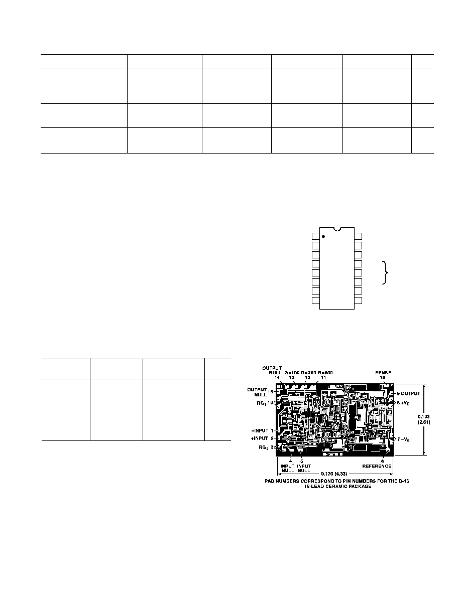
CONNECTION DIAGRAM
–INPUT
+INPUT
RG1
OUTPUT NULL
INPUT NULL
REF
–VS
G = 200
G = 500
SENSE
RG2
INPUT NULL
OUTPUT NULL
G = 100
+VS
OUTPUT
1
2
5
6
7
3
4
8
16
15
12
11
10
14
13
9
TOP VIEW
(Not to Scale)
AD624
SHORT TO
RG2 FOR
DESIRED
GAIN
FOR GAINS OF 1000 SHORT RG1 TO PIN 12
AND PINS 11 AND 13 TO RG2
METALIZATION PHOTOGRAPH
Contact factory for latest dimensions
Dimensions shown in inches and (mm).
ORDERING GUIDE
Temperature
Package
Model
Range
Description
Option
AD624AD
–25
°C to +85°C 16-Lead Ceramic DIP D-16
AD624BD
–25
°C to +85°C 16-Lead Ceramic DIP D-16
AD624CD
–25
°C to +85°C 16-Lead Ceramic DIP D-16
AD624SD
–55
°C to +125°C 16-Lead Ceramic DIP D-16
AD624SD/883B* –55
°C to +125°C 16-Lead Ceramic DIP D-16
AD624AChips
–25
°C to +85°CDie
AD624SChips
–25
°C to +85°CDie
*See Analog Devices’ military data sheet for 883B specifications.
相关PDF资料 |
PDF描述 |
|---|---|
| AD625SD | IC AMP INST 25MHZ LN 16CDIP |
| AD626AR | IC AMP DIFF LP 12MA 8SOIC |
| AD627BR | IC AMP INST R-R 25MA 8SOIC |
| AD628AR-REEL | IC AMP PGA DIFF PREC 8SOIC |
| AD629ARZ-RL | IC AMP DIFF 25MA LDRIFT 8SOIC |
相关代理商/技术参数 |
参数描述 |
|---|---|
| AD624SD/883B | 功能描述:仪表放大器 LOW NOISE PRECISION IN AM RoHS:否 制造商:Texas Instruments 通道数量: 输入补偿电压:150 V 可用增益调整: 最大输入电阻:10 kOhms 共模抑制比(最小值):88 dB 工作电源电压:2.7 V to 36 V 电源电流:200 uA 最大工作温度:+ 125 C 最小工作温度:- 40 C 封装 / 箱体:MSOP-8 封装:Bulk |
| AD625 | 制造商:AD 制造商全称:Analog Devices 功能描述:Programmable Gain Instrumentation Amplifier |
| AD62501P | 制造商:TOSHIBA 制造商全称:Toshiba Semiconductor 功能描述:7 SINGLE DRIVER |
| AD62550A | 制造商:ESMT 制造商全称:Elite Semiconductor Memory Technology Inc. 功能描述:Class-D Audio Power Amplifier with USB / I2S Interface |
| AD62551A | 制造商:ESMT 制造商全称:Elite Semiconductor Memory Technology Inc. 功能描述:USB controller with external Amplifier and Recording function |
发布紧急采购,3分钟左右您将得到回复。