参数资料
| 型号: | AD624SD |
| 厂商: | Analog Devices Inc |
| 文件页数: | 5/17页 |
| 文件大小: | 0K |
| 描述: | IC AMP INST 25MHZ PREC LN 16CDIP |
| 标准包装: | 1 |
| 放大器类型: | 仪表 |
| 电路数: | 1 |
| 转换速率: | 5 V/µs |
| 增益带宽积: | 25MHz |
| -3db带宽: | 1MHz |
| 电流 - 输入偏压: | 50nA |
| 电压 - 输入偏移: | 75µV |
| 电流 - 电源: | 3.5mA |
| 电压 - 电源,单路/双路(±): | ±6 V ~ 18 V |
| 工作温度: | -55°C ~ 125°C |
| 安装类型: | 通孔 |
| 封装/外壳: | 16-CDIP(0.300",7.62mm) |
| 供应商设备封装: | 16-CDIP 侧面铜焊 |
| 包装: | 管件 |
REV. C
AD624
–12–
225.3
124
4445.7
80.2
50
VB
50
20k
10k
AD624
G = 100
G = 200
G = 500
RG1
RG2
–INPUT
(+INPUT)
VOUT
20k
10k
+INPUT
(–INPUT)
AD7528
1/2
AD712
256:1
DATA
INPUTS
CS
WR
DAC A/DAC B
DB0
DB7
+VS
DAC A
DAC B
1/2
AD712
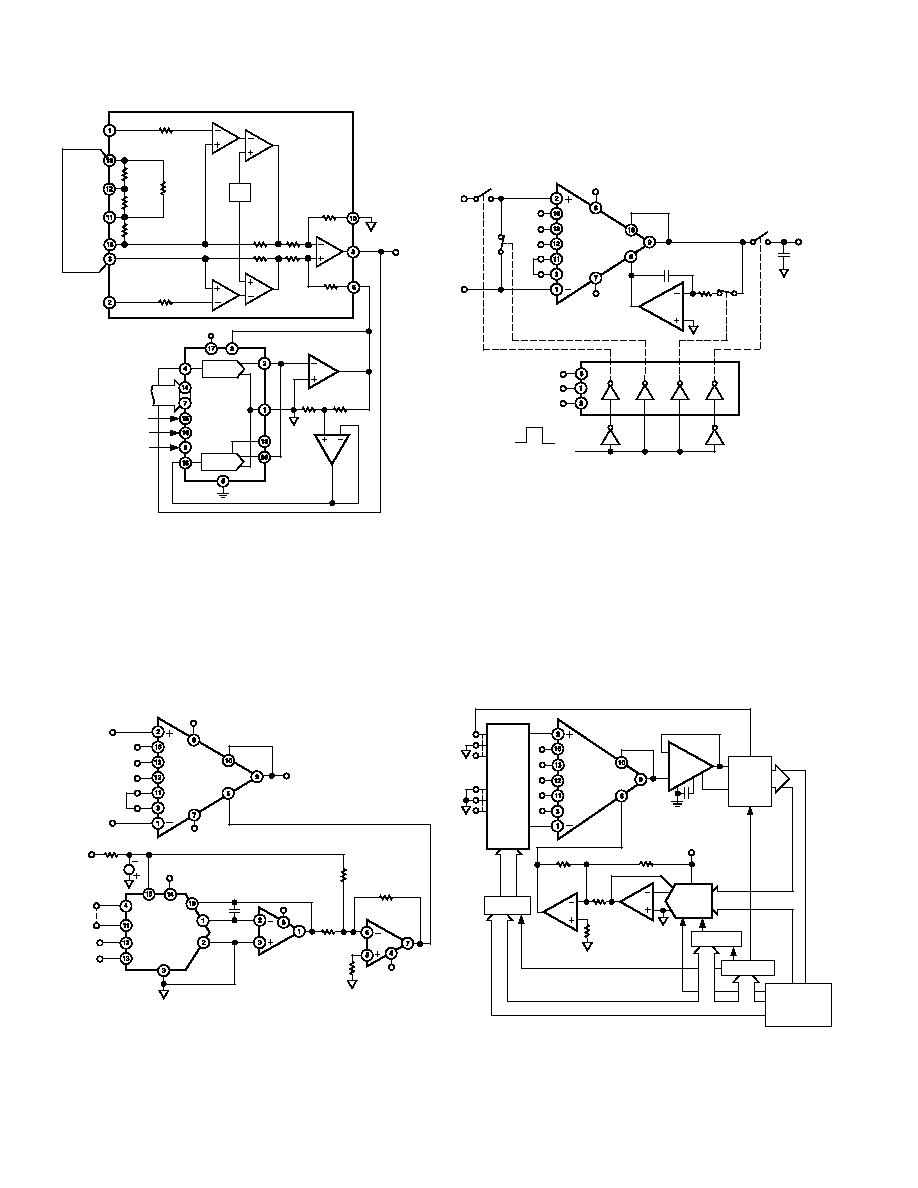
Figure 40. Programmable Output Gain Using a DAC
AUTOZERO CIRCUITS
In many applications it is necessary to provide very accurate
data in high gain configurations. At room temperature the offset
effects can be nulled by the use of offset trimpots. Over the
operating temperature range, however, offset nulling becomes a
problem. The circuit of Figure 41 shows a CMOS DAC operat-
ing in the bipolar mode and connected to the reference terminal
to provide software controllable offset adjustments.
AD624
–VS
+VS
VOUT
G = 100
G = 200
G = 500
RG1
RG2
+INPUT
–INPUT
DATA
INPUTS
CS
WR
MSB
LSB
+VS
AD7524
C1
OUT1
OUT2
1/2
AD712
RFB
+VS
R3
20k
R4
10k
R5
20k
–VS
R6
5k
–VS
GND
AD589
39k
VREF
1/2
AD712
Figure 41. Software Controllable Offset
In many applications complex software algorithms for autozero
applications are not available. For these applications Figure 42
provides a hardware solution.
AD624
–VS
+VS
VOUT
RG1
RG2
1k
12 11
910
0.1 F LOW
LEAKAGE
CH
15
16
14
13
VSS
VDD
GND
A1
A2
A3
A4
AD7510DIKD
200 s
ZERO PULSE
AD542
Figure 42. Autozero Circuit
The microprocessor controlled data acquisition system shown in
Figure 43 includes includes both autozero and autogain capabil-
ity. By dedicating two of the differential inputs, one to ground
and one to the A/D reference, the proper program calibration
cycles can eliminate both initial accuracy errors and accuracy
errors over temperature. The autozero cycle, in this application,
converts a number that appears to be ground and then writes
that same number (8 bit) to the AD624 which eliminates the
zero error since its output has an inverted scale. The autogain
cycle converts the A/D reference and compares it with full scale.
A multiplicative correction factor is then computed and applied
to subsequent readings.
RG1
RG2
AD624
1/2
AD712
AD583
AGND
VIN
VREF
AD574A
AD7507
EN A1
A2
A0
ADDRESS BUS
–VREF
5k
10k
20k
LATCH
20k
1/2
AD712
CONTROL
DECODE
AD7524
MICRO-
PROCESSOR
Figure 43. Microprocessor Controlled Data Acquisition
System
相关PDF资料 |
PDF描述 |
|---|---|
| AD625SD | IC AMP INST 25MHZ LN 16CDIP |
| AD626AR | IC AMP DIFF LP 12MA 8SOIC |
| AD627BR | IC AMP INST R-R 25MA 8SOIC |
| AD628AR-REEL | IC AMP PGA DIFF PREC 8SOIC |
| AD629ARZ-RL | IC AMP DIFF 25MA LDRIFT 8SOIC |
相关代理商/技术参数 |
参数描述 |
|---|---|
| AD624SD/883B | 功能描述:仪表放大器 LOW NOISE PRECISION IN AM RoHS:否 制造商:Texas Instruments 通道数量: 输入补偿电压:150 V 可用增益调整: 最大输入电阻:10 kOhms 共模抑制比(最小值):88 dB 工作电源电压:2.7 V to 36 V 电源电流:200 uA 最大工作温度:+ 125 C 最小工作温度:- 40 C 封装 / 箱体:MSOP-8 封装:Bulk |
| AD625 | 制造商:AD 制造商全称:Analog Devices 功能描述:Programmable Gain Instrumentation Amplifier |
| AD62501P | 制造商:TOSHIBA 制造商全称:Toshiba Semiconductor 功能描述:7 SINGLE DRIVER |
| AD62550A | 制造商:ESMT 制造商全称:Elite Semiconductor Memory Technology Inc. 功能描述:Class-D Audio Power Amplifier with USB / I2S Interface |
| AD62551A | 制造商:ESMT 制造商全称:Elite Semiconductor Memory Technology Inc. 功能描述:USB controller with external Amplifier and Recording function |
发布紧急采购,3分钟左右您将得到回复。