参数资料
| 型号: | AD624SD |
| 厂商: | Analog Devices Inc |
| 文件页数: | 7/17页 |
| 文件大小: | 0K |
| 描述: | IC AMP INST 25MHZ PREC LN 16CDIP |
| 标准包装: | 1 |
| 放大器类型: | 仪表 |
| 电路数: | 1 |
| 转换速率: | 5 V/µs |
| 增益带宽积: | 25MHz |
| -3db带宽: | 1MHz |
| 电流 - 输入偏压: | 50nA |
| 电压 - 输入偏移: | 75µV |
| 电流 - 电源: | 3.5mA |
| 电压 - 电源,单路/双路(±): | ±6 V ~ 18 V |
| 工作温度: | -55°C ~ 125°C |
| 安装类型: | 通孔 |
| 封装/外壳: | 16-CDIP(0.300",7.62mm) |
| 供应商设备封装: | 16-CDIP 侧面铜焊 |
| 包装: | 管件 |
REV. C
AD624
–14–
AD624C
–VS
+VS
G = 100
RG1
RG2
10k
350
+10V
14-BIT
ADC
0 TO 2V
F.S.
350
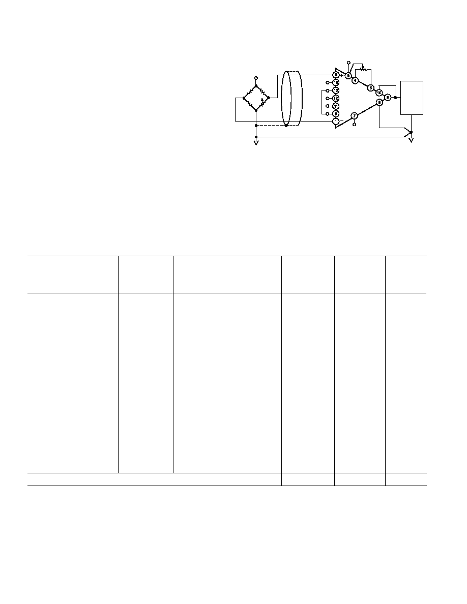
Figure 47. Typical Bridge Application
Table II. Error Budget Analysis of AD624CD in Bridge Application
Effect on
Absolute
Effect
AD624C
Accuracy
on
Error Source
Specifications
Calculation
at TA = +25 C
at TA = +85 C Resolution
Gain Error
±0.1%
±0.1% = 1000 ppm
1000 ppm
–
Gain Instability
10 ppm
(10 ppm/
°C) (60°C) = 600 ppm
_
600 ppm
–
Gain Nonlinearity
±0.001%
±0.001% = 10 ppm
––
10 ppm
Input Offset Voltage
±25 V, RTI
±25 V/20 mV = ±1250 ppm
1250 ppm
–
Input Offset Voltage Drift
±0.25 V/°C(±0.25 V/°C) (60°C)= 15 V
15
V/20 mV = 750 ppm
–
750 ppm
–
Output Offset Voltage
1
±2.0 mV
±2.0 mV/20 mV = 1000 ppm
1000 ppm
–
Output Offset Voltage Drift
1
±10 V/°C(±10 V/°C) (60°C) = 600 V
600
V/20 mV = 300 ppm
–
300 ppm
–
Bias Current–Source
±15 nA
(
±15 nA)(5 ) = 0.075 V
Imbalance Error
0.075
V/20mV = 3.75 ppm
3.75 ppm
–
Offset Current–Source
±10 nA
(
±10 nA)(5 ) = 0.050 V
Imbalance Error
0.050
V/20 mV = 2.5 ppm
2.5 ppm
–
Offset Current–Source
±10 nA
(10 nA) (175
) = 1.75 V
Resistance Error
1.75
V/20 mV = 87.5 ppm
87.5 ppm
–
Offset Current–Source
±100 pA/°C
(100 pA/
°C) (175 ) (60°C) = 1 V
Resistance–Drift
1
V/20 mV = 50 ppm
–
50 ppm
–
Common-Mode Rejection
115 dB
115 dB = 1.8 ppm
× 5V = 9 V
5V dc
9
V/20 mV = 444 ppm
450 ppm
–
Noise, RTI
(0.1 Hz–10 Hz)
0.22
V p-p
0.22
V p-p/20 mV = 10 ppm
_
–
10 ppm
Total Error
3793.75 ppm
5493.75 ppm
20 ppm
NOTE
1Output offset voltage and output offset voltage drift are given as RTI figures.
For a comprehensive study of instrumentation amplifier design
and applications, refer to the Instrumentation Amplifier Application
Guide, available free from Analog Devices.
ERROR BUDGET ANALYSIS
To illustrate how instrumentation amplifier specifications are
applied, we will now examine a typical case where an AD624 is
required to amplify the output of an unbalanced transducer.
Figure 47 shows a differential transducer, unbalanced by
≈5 ,
supplying a 0 to 20 mV signal to an AD624C. The output of the
IA feeds a 14-bit A to D converter with a 0 to 2 volt input volt-
age range. The operating temperature range is –25
°C to +85°C.
Therefore, the largest change in temperature
T within the
operating range is from ambient to +85
°C (85°C – 25°C =
60
°C.)
In many applications, differential linearity and resolution are of
prime importance. This would be so in cases where the absolute
value of a variable is less important than changes in value. In
these applications, only the irreducible errors (20 ppm =
0.002%) are significant. Furthermore, if a system has an intelli-
gent processor monitoring the A to D output, the addition of an
autogain/autozero cycle will remove all reducible errors and may
eliminate the requirement for initial calibration. This will also
reduce errors to 0.002%.
相关PDF资料 |
PDF描述 |
|---|---|
| AD625SD | IC AMP INST 25MHZ LN 16CDIP |
| AD626AR | IC AMP DIFF LP 12MA 8SOIC |
| AD627BR | IC AMP INST R-R 25MA 8SOIC |
| AD628AR-REEL | IC AMP PGA DIFF PREC 8SOIC |
| AD629ARZ-RL | IC AMP DIFF 25MA LDRIFT 8SOIC |
相关代理商/技术参数 |
参数描述 |
|---|---|
| AD624SD/883B | 功能描述:仪表放大器 LOW NOISE PRECISION IN AM RoHS:否 制造商:Texas Instruments 通道数量: 输入补偿电压:150 V 可用增益调整: 最大输入电阻:10 kOhms 共模抑制比(最小值):88 dB 工作电源电压:2.7 V to 36 V 电源电流:200 uA 最大工作温度:+ 125 C 最小工作温度:- 40 C 封装 / 箱体:MSOP-8 封装:Bulk |
| AD625 | 制造商:AD 制造商全称:Analog Devices 功能描述:Programmable Gain Instrumentation Amplifier |
| AD62501P | 制造商:TOSHIBA 制造商全称:Toshiba Semiconductor 功能描述:7 SINGLE DRIVER |
| AD62550A | 制造商:ESMT 制造商全称:Elite Semiconductor Memory Technology Inc. 功能描述:Class-D Audio Power Amplifier with USB / I2S Interface |
| AD62551A | 制造商:ESMT 制造商全称:Elite Semiconductor Memory Technology Inc. 功能描述:USB controller with external Amplifier and Recording function |
发布紧急采购,3分钟左右您将得到回复。