参数资料
| 型号: | AD648JNZ |
| 厂商: | Analog Devices Inc |
| 文件页数: | 12/12页 |
| 文件大小: | 0K |
| 描述: | IC OPAMP BIFET 1MHZ DUAL LP 8DIP |
| 标准包装: | 50 |
| 放大器类型: | J-FET |
| 电路数: | 2 |
| 转换速率: | 1.8 V/µs |
| 增益带宽积: | 1MHz |
| 电流 - 输入偏压: | 5pA |
| 电压 - 输入偏移: | 750µV |
| 电流 - 电源: | 340µA |
| 电流 - 输出 / 通道: | 15mA |
| 电压 - 电源,单路/双路(±): | ±4.5 V ~ 18 V |
| 工作温度: | 0°C ~ 70°C |
| 安装类型: | 通孔 |
| 封装/外壳: | 8-DIP(0.300",7.62mm) |
| 供应商设备封装: | 8-PDIP |
| 包装: | 管件 |
| 产品目录页面: | 773 (CN2011-ZH PDF) |
AD648
REV. E
–9–
TEMP
RSH
VOS
IB
C(M )( V)
(1 + RF/RSH) VOS
(pA)
IBRF
TOTAL
–25
15,970
150
151
V
0.30
30
V
181
V
0
2,830
225
233
V
2.26
262
V
495
V
+25
500
300
360
V
10.00
1.0 mV
1.36 mV
+50
88.5
375
800
V
56.6
5.6 mV
6.40 mV
+75
15.6
450
3.33 mV
320
32 mV
35.3 mV
+85
7.8
480
6.63 mV
640
64 mV
70.6 mV
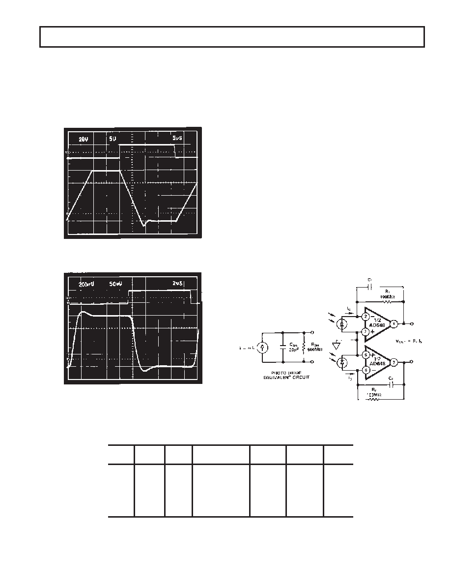
Figure 28. Photodiode Pre-Amp Errors Over Temperature
DUAL PHOTODIODE PREAMP
The performance of the dual photodiode preamp shown in
Figure 27 is enhanced by the AD648’s low input current, input
voltage offset, and offset voltage drift. Each photodiode sources
a current proportional to the incident light power on its surface.
RF converts the photodiode current to an output voltage equal
to RF
× IS.
An error budget illustrating the importance of low amplifier
input current, voltage offset, and offset voltage drift to minimize
output voltage errors can be developed by considering the
equivalent circuit for the small (0.2 mm
2 area) photodiode
shown in Figure 27. The input current results in an error pro-
portional to the feedback resistance used. The amplifier’s offset
will produce an error proportional to the preamp’s noise gain
(1+RF/RSH), where RSH is the photodiode shunt resistance. The
amplifier’s input current will double with every 10
°C rise in
temperature, and the photodiode’s shunt resistance halves with
every 10
°C rise. The error budget in Figure 28 assumes a room
temperature photodiode RSH of 500 M
, and the maximum
input current and input offset voltage specs of an AD648C.
The capacitance at the amplifier’s negative input (the sum of the
photodiode’s shunt capacitance, the op amp’s differential input
capacitance, stray capacitance due to wiring, etc.) will cause a
rise in the preamp’s noise gain over frequency. This can result in
excess noise over the bandwidth of interest. CF reduces the
noise gain “peaking” at the expense of signal bandwidth.
Figure 27. A Dual Photodiode Pre-Amp
The AD648 in this configuration provides a 700 kHz small signal
bandwidth and 1.8 V/
s typical slew rate. The 33 pF capacitor
across the feedback resistor optimizes the circuit’s response. The
oscilloscope photos in Figures 26a and 26b show small and
large signal outputs of the circuit in Figure 24. Upper traces
show the input signal VIN. Lower traces are the resulting output
voltage with the DAC’s digital input set to all 1s. The circuit
settles to
±0.01% for a 20 V input step in 14 s.
Figure 26a. Response to
±20 V p-p Reference Square
Wave
Figure 26b. Response to
±100 mV p-p Reference Square
Wave
相关PDF资料 |
PDF描述 |
|---|---|
| TSW-123-06-T-S | CONN HEADER 23POS .100" SNGL TIN |
| TSW-123-05-T-S | CONN HEADER 23POS .100" SNGL TIN |
| BK/AGC-1/32 | FUSE 1/32A 250V FAST AGC GLASS |
| 9-146282-0-21 | CONN HDR BRKWAY .100 21POS VERT |
| 4-103741-0-21 | CONN HEADR BRKWAY .100 21POS STR |
相关代理商/技术参数 |
参数描述 |
|---|---|
| AD648JNZKL1 | 制造商:Rochester Electronics LLC 功能描述: 制造商:Analog Devices 功能描述: |
| AD648JR | 制造商:Analog Devices 功能描述:OP Amp Dual GP ±18V 8-Pin SOIC N 制造商:Rochester Electronics LLC 功能描述:LOW POWER DUAL OP AMP IC - Bulk 制造商:Analog Devices 功能描述:IC OP-AMP DUAL BIFET |
| AD648JR-REEL | 制造商:Analog Devices 功能描述:OP Amp Dual GP ±18V 8-Pin SOIC N T/R |
| AD648JR-REEL7 | 制造商:Analog Devices 功能描述:OP Amp Dual GP ±18V 8-Pin SOIC N T/R |
| AD648JRZ | 功能描述:IC OPAMP BIFET 1MHZ DUAL 8SOIC RoHS:是 类别:集成电路 (IC) >> Linear - Amplifiers - Instrumentation 系列:- 产品培训模块:Differential Circuit Design Techniques for Communication Applications 标准包装:1 系列:- 放大器类型:RF/IF 差分 电路数:1 输出类型:差分 转换速率:9800 V/µs 增益带宽积:- -3db带宽:2.9GHz 电流 - 输入偏压:3µA 电压 - 输入偏移:- 电流 - 电源:40mA 电流 - 输出 / 通道:- 电压 - 电源,单路/双路(±):3 V ~ 3.6 V 工作温度:-40°C ~ 85°C 安装类型:表面贴装 封装/外壳:16-VQFN 裸露焊盘,CSP 供应商设备封装:16-LFCSP-VQ 包装:剪切带 (CT) 产品目录页面:551 (CN2011-ZH PDF) 其它名称:ADL5561ACPZ-R7CT |
发布紧急采购,3分钟左右您将得到回复。