参数资料
| 型号: | AD6623ASZ |
| 厂商: | Analog Devices Inc |
| 文件页数: | 1/48页 |
| 文件大小: | 0K |
| 描述: | IC TSP 4CHAN 104MSPS 128MQFP |
| 标准包装: | 1 |
| 应用: | 传输信息处理器 |
| 接口: | 串行 |
| 封装/外壳: | 128-BFQFP |
| 供应商设备封装: | 128-MQFP(14x20) |
| 包装: | 托盘 |
| 安装类型: | 表面贴装 |
当前第1页第2页第3页第4页第5页第6页第7页第8页第9页第10页第11页第12页第13页第14页第15页第16页第17页第18页第19页第20页第21页第22页第23页第24页第25页第26页第27页第28页第29页第30页第31页第32页第33页第34页第35页第36页第37页第38页第39页第40页第41页第42页第43页第44页第45页第46页第47页第48页
REV. A
Information furnished by Analog Devices is believed to be accurate and
reliable. However, no responsibility is assumed by Analog Devices for its
use, nor for any infringements of patents or other rights of third parties that
may result from its use. No license is granted by implication or otherwise
under any patent or patent rights of Analog Devices.
a
AD6623
One Technology Way, P.O. Box 9106, Norwood, MA 02062-9106, U.S.A.
Tel: 781/329-4700
Fax: 781/326-8703
Analog Devices, Inc., 2002
4-Channel, 104 MSPS Digital
Transmit Signal Processor (TSP)
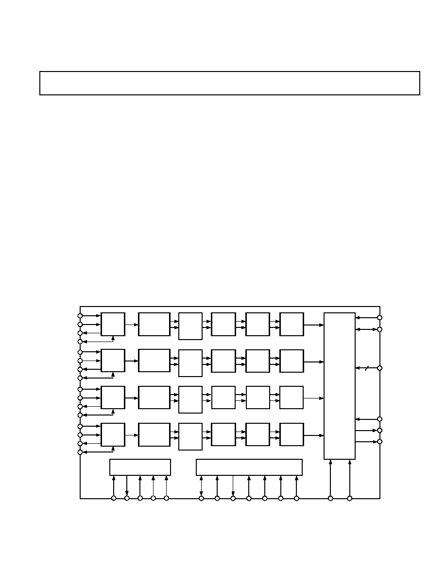
FUNCTIONAL BLOCK DIAGRAM
SPORT
RAM
COEFFICIENT
FILTER
DATA
SCALER
AND
POWER
RAMP
CIC5
FILTER
rCIC2
FILTER
NCO
I
Q
CHAN A
I
Q
I
Q
I
Q
JTAG
CS
A[2:0]
MODE
RW
DTACK
DS
D[7:0]
IN
QIN
SYNC
OEN
QOUT
OUT
[17:0]
SDINA
SDFIA
SDFOA
SCLKA
SDINB
SDFIB
SDFOB
SCLKB
SDINC
SDFIC
SDFOC
SCLKC
SDIND
SDFID
SCLKD
SDFOD
SUMMATION
SCALER
AND
POWER
RAMP
CIC5
FILTER
rCIC2
FILTER
NCO
I
Q
CHAN B
I
Q
I
Q
I
Q
SCALER
AND
POWER
RAMP
CIC5
FILTER
rCIC2
FILTER
NCO
I
Q
CHAN C
I
Q
I
Q
I
Q
SCALER
AND
POWER
RAMP
CIC5
FILTER
rCIC2
FILTER
NCO
I
Q
CHAN D
I
Q
I
Q
I
Q
MICROPORT
CLK
RESET
4
[17–0]
SPORT
RAM
COEFFICIENT
FILTER
DATA
SPORT
RAM
COEFFICIENT
FILTER
DATA
SPORT
RAM
COEFFICIENT
FILTER
DATA
NCO = NUMERICALLY CONTROLLED
OSCILLATOR/TUNER
TDL
TMS TCK
TRST
TDO
FEATURES
Pin Compatible to the AD6622
18-Bit Parallel Digital IF Output
Real or Interleaved Complex
18-Bit Bidirectional Parallel Digital IF Input/Output
Allows Cascade of Chips for Additional Channels
Clipped or Wrapped Over Range
Two’s Complement or Offset Binary Output
Four Independent Digital Transmitters in Single Package
RAM Coefficient Filter (RCF)
Programmable IF and Modulation for Each Channel
Programmable Interpolating RAM Coefficient Filter
/4-DQPSK Differential Phase Encoder
3 /8-PSK Linear Encoder
8-PSK Linear Encoder
Programmable GMSK Look-Up Table
Programmable QPSK Look-Up Table
All-Pass Phase Equalizer
Programmable Fine Scaler
Programmable Power Ramp Unit
High Speed CIC Interpolating Filter
Digital Resampling for Noninteger Interpolation Rates
NCO Frequency Translation
Carrier Output from DC to 52 MHz
Spurious Performance Better than –100 dBc
Separate 3-Wire Serial Data Input for Each Channel
Bidirectional Serial Clocks and Frames
Microprocessor Control
2.5 V CMOS Core, 3.3 V Outputs, 5 V Inputs
JTAG Boundary Scan
APPLICATIONS
Cellular/PCS Base Stations
Micro/Pico Cell Base Stations
Wireless Local Loop Base Stations
Multicarrier, Multimode Digital Transmit
GSM, EDGE, IS136, PHS, IS95, TDS CDMA, UMTS,
CDMA2000
Phased Array Beam Forming Antennas
Software Defined Radio
Tuning Resolution Better than 0.025 Hz
Real or Complex Outputs
相关PDF资料 |
PDF描述 |
|---|---|
| AD6641BCPZRL7-500 | IC IF RCVR 11BIT 200MSPS 56LFCSP |
| AD664BJ | IC DAC 12BIT QUAD MONO 44-JLCC |
| AD667BD | IC DAC 12BIT W/BUFF LTCH 28-CDIP |
| AD669BN | IC DAC 16BIT MONO VREF 28-DIP |
| AD693AE | IC SGNL COND 4-20MA TX 20-CLCC |
相关代理商/技术参数 |
参数描述 |
|---|---|
| AD6623BC/PCB | 制造商:AD 制造商全称:Analog Devices 功能描述:4-Channel, 104 MSPS Digital Transmit Signal Processor TSP |
| AD6623PCB | 制造商:AD 制造商全称:Analog Devices 功能描述:4-Channel, 104 MSPS Digital Transmit Signal Processor TSP |
| AD6623S/PCB | 制造商:Analog Devices 功能描述:4-CH, 104 MSPS DGTL TRANSMIT SGNL PROCESSOR (TSP) 28SOIC - Bulk |
| AD6624 | 制造商:AD 制造商全称:Analog Devices 功能描述:Four-Channel, 80 MSPS Digital Receive Signal Processor (RSP) |
| AD6624A | 制造商:AD 制造商全称:Analog Devices 功能描述:Four-Channel, 100 MSPS Digital Receive Signal Processor (RSP) |
发布紧急采购,3分钟左右您将得到回复。