参数资料
| 型号: | AD664JNZ-UNI |
| 厂商: | Analog Devices Inc |
| 文件页数: | 11/23页 |
| 文件大小: | 0K |
| 描述: | IC DAC 12BIT QUAD UNIPOL 28DIP |
| 产品培训模块: | Data Converter Fundamentals DAC Architectures |
| 标准包装: | 1 |
| 设置时间: | 8µs |
| 位数: | 12 |
| 数据接口: | 并联 |
| 转换器数目: | 4 |
| 电压电源: | 双 ± |
| 功率耗散(最大): | 525mW |
| 工作温度: | 0°C ~ 70°C |
| 安装类型: | 通孔 |
| 封装/外壳: | 28-DIP(0.600",15.24mm) |
| 供应商设备封装: | 28-PDIP |
| 包装: | 管件 |
| 输出数目和类型: | 4 电压,单极;4 电压,双极 |
| 采样率(每秒): | 125k |
AD664
REV.
–19–
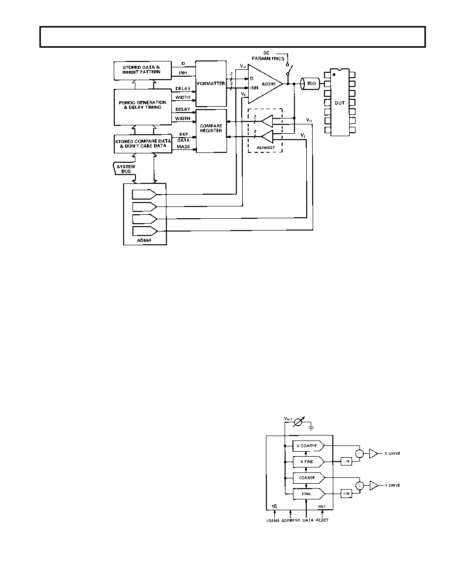
Figure 29. AD664 in “Tester-per-Pin” Architecture
APPLICATIONS OF THE AD664
“Tester-Per-Pin” ATE Architecture
Figure 29 shows the AD664 used in a single channel of a digital
test system. In this scheme, the AD664 supplies four individual
output voltages. Two are provided to the VHIGH and VLOW in-
puts of the AD345 pin driver I.C. to set the digital output levels.
Two others are routed to the inputs of the AD96687 dual com-
parator to supply reference levels of the readback features. This
approach can be replicated to give as many channels of stimulus/
readback as the tester has pins. The AD664 is a particularly
appropriate choice for a large-scale system because the low
power requirements (under 500 mW) ease power supply and
cooling requirements. Analog ground currents of 600
A or less
make the ground current management task simpler. All DACs
can be driven from the same system reference and will track
over time and temperature. Finally, the small board area
required by the AD664 (and AD345 and AD96687) allows a
high functional density.
X-Y Plotters
Figure 30 is a block diagram of the control section of a
microprocessor-controlled X-Y pen plotter. In this conceptual
exercise, two of the DACs are used for the X-channel drive and
two are used for the Y-channel drive. Each provides either the
coarse or fine movement control for its respective channel. This
approach offers increased resolution over some other approaches.
A designer can take advantage of the reset feature of the AD664
in the following manner. If the system is designed such that the
“HOME” position of the pen (or galvanometer, beam, head or
similar mechanism) results when the outputs of all of the DACs
are at zero, then no system software is required to home the
pen. A simple reset signal is sufficient.
Similarly, the transparent feature could be used to the same
end. One code can be sent to all DACs at the same time to send
the pen to the home position. Of course, this would require
some software where the previous example would require only a
single reset strobe signal!
Drawing scaling can be achieved by taking advantage of the
AD664’s software programmable gain settings. If, for example,
an “A” size drawing is created with gain settings of 1, then a
“C” size drawing can be created by simply resetting all DAC
gains to 2 and redrawing the object. Conversely, a “C” size
drawing created with gains of 2 can be reduced to “A” size sim-
ply by changing the gains to 1 and redrawing. The same princi-
pal applies for conversion from “B” size to “D” size or “D” size
to “B” size. The multiplying capability of the AD664 provides
another scaling option. Changing the reference voltage provides
a proportional change in drawing size. Inverting the reference
voltage would invert the drawing.
Swapping digital input data from the X channel to the Y chan-
nel would rotate the drawing 90 degrees.
Figure 30. X-Y Plotter Block Diagram
D
相关PDF资料 |
PDF描述 |
|---|---|
| AD5370BSTZ-REEL | IC DAC 16BIT 40CH SERIAL 64-LQFP |
| AD5370BCPZ-REEL7 | IC DAC 16BIT 40CH SERIAL 64LFCSP |
| VE-J5P-MW-S | CONVERTER MOD DC/DC 13.8V 100W |
| AD75004KPZ | IC DAC 12BIT QUAD W/BUFF 28-PLCC |
| AD7228LPZ | IC DAC 8BIT OCTAL W/AMP 28-PLCC |
相关代理商/技术参数 |
参数描述 |
|---|---|
| AD664JP | 功能描述:IC DAC 12BIT QUAD MONO 44-PLCC RoHS:否 类别:集成电路 (IC) >> 数据采集 - 数模转换器 系列:- 产品培训模块:Lead (SnPb) Finish for COTS Obsolescence Mitigation Program 标准包装:1,000 系列:- 设置时间:1µs 位数:8 数据接口:串行 转换器数目:8 电压电源:双 ± 功率耗散(最大):941mW 工作温度:0°C ~ 70°C 安装类型:表面贴装 封装/外壳:24-SOIC(0.295",7.50mm 宽) 供应商设备封装:24-SOIC W 包装:带卷 (TR) 输出数目和类型:8 电压,单极 采样率(每秒):* |
| AD664JPZ | 功能描述:IC DAC 12BIT QUAD MONO 44-PLCC RoHS:是 类别:集成电路 (IC) >> 数据采集 - 数模转换器 系列:- 产品培训模块:Lead (SnPb) Finish for COTS Obsolescence Mitigation Program 标准包装:1,000 系列:- 设置时间:1µs 位数:8 数据接口:串行 转换器数目:8 电压电源:双 ± 功率耗散(最大):941mW 工作温度:0°C ~ 70°C 安装类型:表面贴装 封装/外壳:24-SOIC(0.295",7.50mm 宽) 供应商设备封装:24-SOIC W 包装:带卷 (TR) 输出数目和类型:8 电压,单极 采样率(每秒):* |
| AD664KN-BIP | 功能描述:IC DAC 12BIT QUAD BIPOLAR 28-DIP RoHS:否 类别:集成电路 (IC) >> 数据采集 - 数模转换器 系列:- 产品培训模块:Lead (SnPb) Finish for COTS Obsolescence Mitigation Program 标准包装:1,000 系列:- 设置时间:1µs 位数:8 数据接口:串行 转换器数目:8 电压电源:双 ± 功率耗散(最大):941mW 工作温度:0°C ~ 70°C 安装类型:表面贴装 封装/外壳:24-SOIC(0.295",7.50mm 宽) 供应商设备封装:24-SOIC W 包装:带卷 (TR) 输出数目和类型:8 电压,单极 采样率(每秒):* |
| AD664KN-UNI | 功能描述:IC DAC 12BIT QUAD UNIPOL 28-DIP RoHS:否 类别:集成电路 (IC) >> 数据采集 - 数模转换器 系列:- 标准包装:2,400 系列:- 设置时间:- 位数:18 数据接口:串行 转换器数目:3 电压电源:模拟和数字 功率耗散(最大):- 工作温度:-40°C ~ 85°C 安装类型:表面贴装 封装/外壳:36-TFBGA 供应商设备封装:36-TFBGA 包装:带卷 (TR) 输出数目和类型:* 采样率(每秒):* |
| AD664KNZ-BIP | 功能描述:IC DAC 12BIT QUAD BIPOLAR 28DIP RoHS:是 类别:集成电路 (IC) >> 数据采集 - 数模转换器 系列:- 产品培训模块:Lead (SnPb) Finish for COTS Obsolescence Mitigation Program 标准包装:1,000 系列:- 设置时间:1µs 位数:8 数据接口:串行 转换器数目:8 电压电源:双 ± 功率耗散(最大):941mW 工作温度:0°C ~ 70°C 安装类型:表面贴装 封装/外壳:24-SOIC(0.295",7.50mm 宽) 供应商设备封装:24-SOIC W 包装:带卷 (TR) 输出数目和类型:8 电压,单极 采样率(每秒):* |
发布紧急采购,3分钟左右您将得到回复。