参数资料
| 型号: | AD664JNZ-UNI |
| 厂商: | Analog Devices Inc |
| 文件页数: | 21/23页 |
| 文件大小: | 0K |
| 描述: | IC DAC 12BIT QUAD UNIPOL 28DIP |
| 产品培训模块: | Data Converter Fundamentals DAC Architectures |
| 标准包装: | 1 |
| 设置时间: | 8µs |
| 位数: | 12 |
| 数据接口: | 并联 |
| 转换器数目: | 4 |
| 电压电源: | 双 ± |
| 功率耗散(最大): | 525mW |
| 工作温度: | 0°C ~ 70°C |
| 安装类型: | 通孔 |
| 封装/外壳: | 28-DIP(0.600",15.24mm) |
| 供应商设备封装: | 28-PDIP |
| 包装: | 管件 |
| 输出数目和类型: | 4 电压,单极;4 电压,双极 |
| 采样率(每秒): | 125k |
AD664
REV.
–7–
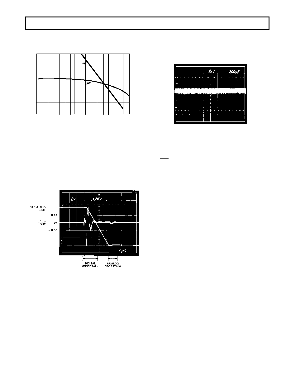
Multiplying Mode Performance
Figure 6 illustrates the typical open-loop gain and phase perfor-
mance of the output amplifiers of the AD664.
GAIN
–
dB
0
+5
+20
+15
+10
10k
100k
1M
0
+45
+90
PHASE
MARGIN
–
Degrees
FREQUENCY – H z
GAIN
PHASE
Figure 6. Gain and Phase Performance of AD664 Outputs
Crosstalk
Crosstalk is a spurious signal on one DAC output caused by a
change in the output of one or more of the other DACs.
Crosstalk can be induced by capacitive, thermal or load current
induced feedthrough. Figure 7 shows typical crosstalk. DAC B
is set to output 0 volts. The outputs of DAC A, C and D switch
2 k
loads from 10 V to 0 V. The first disturbance in the output
of DAC B is caused by digital feedthrough from the input data
lows. The second disturbance is caused by analog feedthrough
from the other DAC outputs.
Figure 7. Output Crosstalk
Output Noise
Wideband output noise is shown in Figure 8. This measurement
was made with a 7 MHz noise bandwidth, gain = 1 and all bits
on. The total rms noise is approximately one fifth the visual
peak-to-peak noise.
DIGITAL INTERFACE
As Table II shows, the AD664 makes a wide variety of operating
modes available to the user. These modes are accessed or pro-
grammed through the high speed digital port of the quad DAC.
On-board registers program and store the DAC input codes and
the DAC operating mode data. All registers are double-buffered
to allow for simultaneous updating of all outputs. Register data
may be read back to verify the respective contents. The digital
port also allows transparent operation. Data from the input pins
can be sent directly through both ranks of latches to the DAC.
Figure 8. Typical Output Noise
Partial address decoding is performed by the DS0, DS1, QS0,
QS1
and QS2 address bits. QS0, QS1 and QS2 allow the 44-pin
versions of the AD664 to be addressed in 4-bit nibble, 8-bit byte
or 12-bit parallel words.
The RST pin provides a simple method to reset all output
voltages to zero. Its advantages are speed and low software
overhead.
INPUT DATA
In general, two types of data will be input to the registers of the
AD664, input code data and mode select data. Input code data
sets the DAC inputs while the mode select data sets the gain
and range of each DAC.
The versatile I/O port of the AD664 allows many different types
of data input schemes. For example, the input code for just one
of the DACs may be loaded and the output may or may not be
updated. Or, the input codes for all four DACs may be written,
and the outputs may or may not be updated.
The same applies for MODE SELECTION. The mode of just
one or many of the DACs may be rewritten and the user can
choose to immediately update the outputs or wait until a later
time to transfer the mode information to the outputs.
A user may also write both input code and mode information
into their respective first ranks and then update all second ranks
at once.
Finally, transparent operation allows data to be transferred from
the inputs to the outputs using a single control line. This feature
is useful, for example, in a situation where one of the DACs is
used in an A/D converter. The SAR register could be connected
directly to a DAC by using the transparent mode of operation.
Another use for this feature would be during system calibration
where the endpoints of the transfer function of each DAC would
be measured. For example, if the full-scale voltages of each
DAC were to be measured, then by making all four DACs
transparent and putting all “1s” on the input port, all four
DACs would be at full-scale. This requires far less software
overhead than loading each register individually.
D
相关PDF资料 |
PDF描述 |
|---|---|
| AD5370BSTZ-REEL | IC DAC 16BIT 40CH SERIAL 64-LQFP |
| AD5370BCPZ-REEL7 | IC DAC 16BIT 40CH SERIAL 64LFCSP |
| VE-J5P-MW-S | CONVERTER MOD DC/DC 13.8V 100W |
| AD75004KPZ | IC DAC 12BIT QUAD W/BUFF 28-PLCC |
| AD7228LPZ | IC DAC 8BIT OCTAL W/AMP 28-PLCC |
相关代理商/技术参数 |
参数描述 |
|---|---|
| AD664JP | 功能描述:IC DAC 12BIT QUAD MONO 44-PLCC RoHS:否 类别:集成电路 (IC) >> 数据采集 - 数模转换器 系列:- 产品培训模块:Lead (SnPb) Finish for COTS Obsolescence Mitigation Program 标准包装:1,000 系列:- 设置时间:1µs 位数:8 数据接口:串行 转换器数目:8 电压电源:双 ± 功率耗散(最大):941mW 工作温度:0°C ~ 70°C 安装类型:表面贴装 封装/外壳:24-SOIC(0.295",7.50mm 宽) 供应商设备封装:24-SOIC W 包装:带卷 (TR) 输出数目和类型:8 电压,单极 采样率(每秒):* |
| AD664JPZ | 功能描述:IC DAC 12BIT QUAD MONO 44-PLCC RoHS:是 类别:集成电路 (IC) >> 数据采集 - 数模转换器 系列:- 产品培训模块:Lead (SnPb) Finish for COTS Obsolescence Mitigation Program 标准包装:1,000 系列:- 设置时间:1µs 位数:8 数据接口:串行 转换器数目:8 电压电源:双 ± 功率耗散(最大):941mW 工作温度:0°C ~ 70°C 安装类型:表面贴装 封装/外壳:24-SOIC(0.295",7.50mm 宽) 供应商设备封装:24-SOIC W 包装:带卷 (TR) 输出数目和类型:8 电压,单极 采样率(每秒):* |
| AD664KN-BIP | 功能描述:IC DAC 12BIT QUAD BIPOLAR 28-DIP RoHS:否 类别:集成电路 (IC) >> 数据采集 - 数模转换器 系列:- 产品培训模块:Lead (SnPb) Finish for COTS Obsolescence Mitigation Program 标准包装:1,000 系列:- 设置时间:1µs 位数:8 数据接口:串行 转换器数目:8 电压电源:双 ± 功率耗散(最大):941mW 工作温度:0°C ~ 70°C 安装类型:表面贴装 封装/外壳:24-SOIC(0.295",7.50mm 宽) 供应商设备封装:24-SOIC W 包装:带卷 (TR) 输出数目和类型:8 电压,单极 采样率(每秒):* |
| AD664KN-UNI | 功能描述:IC DAC 12BIT QUAD UNIPOL 28-DIP RoHS:否 类别:集成电路 (IC) >> 数据采集 - 数模转换器 系列:- 标准包装:2,400 系列:- 设置时间:- 位数:18 数据接口:串行 转换器数目:3 电压电源:模拟和数字 功率耗散(最大):- 工作温度:-40°C ~ 85°C 安装类型:表面贴装 封装/外壳:36-TFBGA 供应商设备封装:36-TFBGA 包装:带卷 (TR) 输出数目和类型:* 采样率(每秒):* |
| AD664KNZ-BIP | 功能描述:IC DAC 12BIT QUAD BIPOLAR 28DIP RoHS:是 类别:集成电路 (IC) >> 数据采集 - 数模转换器 系列:- 产品培训模块:Lead (SnPb) Finish for COTS Obsolescence Mitigation Program 标准包装:1,000 系列:- 设置时间:1µs 位数:8 数据接口:串行 转换器数目:8 电压电源:双 ± 功率耗散(最大):941mW 工作温度:0°C ~ 70°C 安装类型:表面贴装 封装/外壳:24-SOIC(0.295",7.50mm 宽) 供应商设备封装:24-SOIC W 包装:带卷 (TR) 输出数目和类型:8 电压,单极 采样率(每秒):* |
发布紧急采购,3分钟左右您将得到回复。