参数资料
| 型号: | AD664JNZ-UNI |
| 厂商: | Analog Devices Inc |
| 文件页数: | 3/23页 |
| 文件大小: | 0K |
| 描述: | IC DAC 12BIT QUAD UNIPOL 28DIP |
| 产品培训模块: | Data Converter Fundamentals DAC Architectures |
| 标准包装: | 1 |
| 设置时间: | 8µs |
| 位数: | 12 |
| 数据接口: | 并联 |
| 转换器数目: | 4 |
| 电压电源: | 双 ± |
| 功率耗散(最大): | 525mW |
| 工作温度: | 0°C ~ 70°C |
| 安装类型: | 通孔 |
| 封装/外壳: | 28-DIP(0.600",15.24mm) |
| 供应商设备封装: | 28-PDIP |
| 包装: | 管件 |
| 输出数目和类型: | 4 电压,单极;4 电压,双极 |
| 采样率(每秒): | 125k |
AD664
REV.
–11–
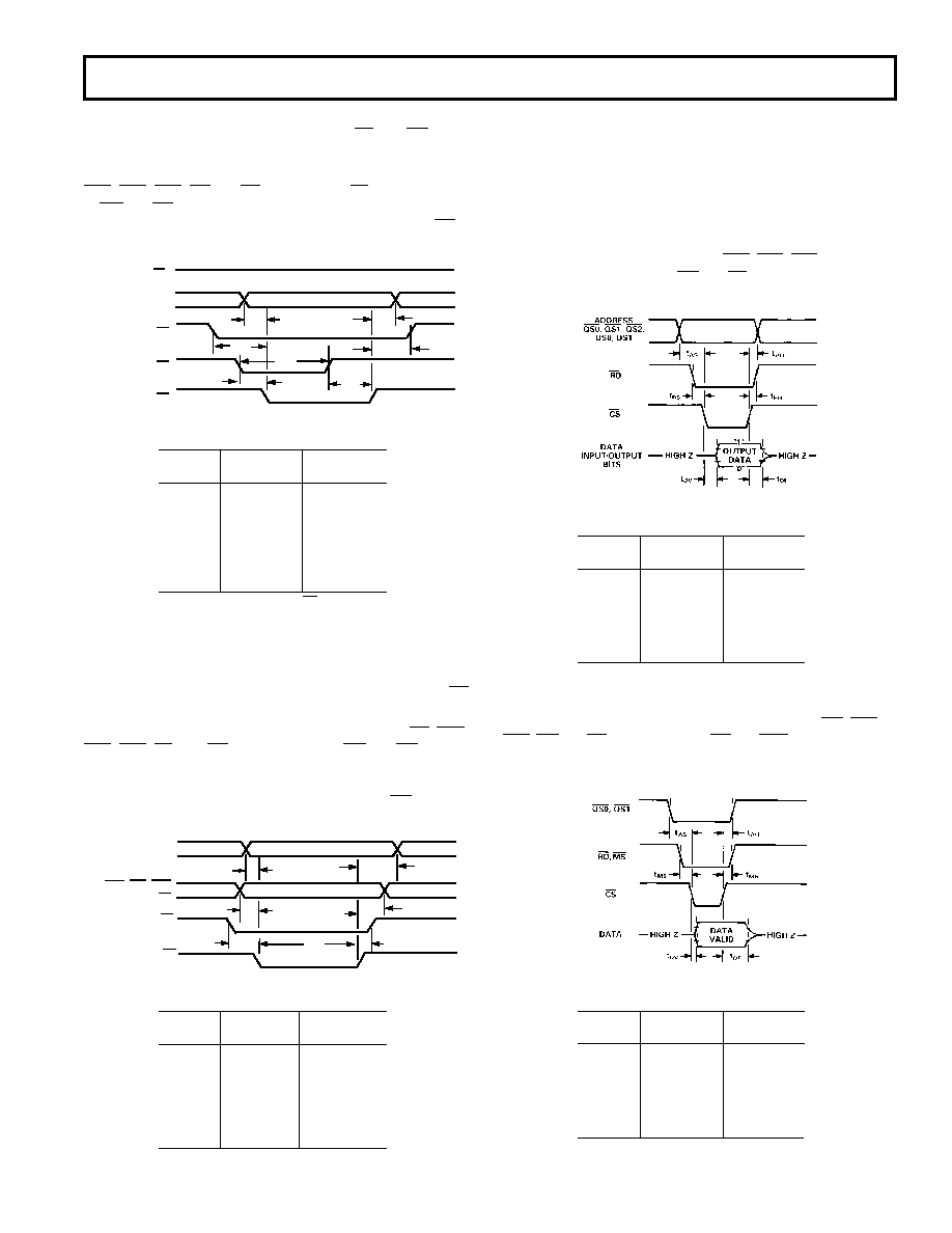
OUTPUT DATA
Two types of outputs may be obtained from the internal data
registers of the AD664 chip, mode select and DAC input code
data. Readback data may be in the same forms in which it can
be entered; 4-, 8-, and 12-bit wide words (12 bits only for
28-pin versions).
DAC Data Readback
DAC input code readback data is obtained by setting the address
of the DAC (DS0, DS1) and Quads (QS0, QS1, QS2) on the
address pins and bringing the RD and CS pins low. The timing
diagram for a DAC code readback operation appears in Figure 20.
Figure 20a. DAC Input Code Readback
25
°CT
MIN to TMAX
SYMBOL
MIN (ns)
tAS
00
tRS
00
tDV
150
180
tDF
60
75
tAH
00
tRH
00
Figure 20b. DAC Input Code Readback Timing
Mode Data Readback
Mode data is read back in a similar fashion. By setting MS, QS0,
QS1
, RD and CS low while setting TR and RST high, the mode
select word is presented to the I/O port pins. Figure 21 shows the
timing diagram for a readback of the mode select data register.
Figure 21a. Mode Data Readback
25 CTMIN to TMAX
SYMBOL
MIN (ns)
tAS
00
tMS
00
tDV
150
180
tDF
60
75
tAH
00
tMH
00
Figure 21b. DAC Mode Readback Timing
Fully transparent operation can be thought of as a simultaneous
load of data from Figure 9a where replacing LS with TR causes
all 4 DACs to be loaded at once.
The Fully transparent mode is achieved by asserting lows on
QS0
, QS1, QS2, TR and CS while keeping LS high in addition
to MS and RB. Figure 18a illustrates the necessary timing rela-
tionships. Fully transparent operation will also work with TR
tied low (enabled).
DATA INPUT/
OUTPUT BITS
tTS
t
DS
t
QH
tDH
t
QS
DATA VALID
TW
t
CH
1
LS
QS
TR
CS
Figure 18a. Fully Transparent Mode
25 CTMIN to TMAX
SYMBOL
MIN (ns)
tAS
00
tQS
00
tTS*0
0
tTW
80
90
tCH
90
110
tDH
00
tQH
00
*FOR tTS > 0, THE WIDTH OF TR MUST BE
INCREASED BY THE SAME AMOUNT THAT
tTS IS GREATER THAN 0 ns.
Figure 18b. Fully Transparent Mode Timing
Partially transparent operation can be thought of as preloading
the first rank in Figure 10a without requiring the additional CS
pulse from Figure 11.
The partially transparent mode is achieved by setting CS, QS0,
QS1
, QS2, LS, and TR low while keeping RD and MS high.
The address of the transparent DAC is asserted on DS0 and
DS1. Figure 19a illustrates the necessary timing relationships.
Partially transparent operation will also work with TR tied low
(enabled).
DATA INPUT/
OUTPUT BITS
ADDRESS
QS0, QS1, QS2
DS0, DS1, LS
tTS
t
AS
t
DH
DATA VALID
W
t
tTH
TR
CS
ADDRESS VALID
tAH
t
DS
Figure 19a. Partially Transparent
25
°CT
MIN to TMAX
SYMBOL
MIN (ns)
tDS
00
tAS
00
tTS
00
tW
90
110
tDH
15
tAH
15
tTH
15
Figure 19b. Partially Transparent Mode Timing
D
相关PDF资料 |
PDF描述 |
|---|---|
| AD5370BSTZ-REEL | IC DAC 16BIT 40CH SERIAL 64-LQFP |
| AD5370BCPZ-REEL7 | IC DAC 16BIT 40CH SERIAL 64LFCSP |
| VE-J5P-MW-S | CONVERTER MOD DC/DC 13.8V 100W |
| AD75004KPZ | IC DAC 12BIT QUAD W/BUFF 28-PLCC |
| AD7228LPZ | IC DAC 8BIT OCTAL W/AMP 28-PLCC |
相关代理商/技术参数 |
参数描述 |
|---|---|
| AD664JP | 功能描述:IC DAC 12BIT QUAD MONO 44-PLCC RoHS:否 类别:集成电路 (IC) >> 数据采集 - 数模转换器 系列:- 产品培训模块:Lead (SnPb) Finish for COTS Obsolescence Mitigation Program 标准包装:1,000 系列:- 设置时间:1µs 位数:8 数据接口:串行 转换器数目:8 电压电源:双 ± 功率耗散(最大):941mW 工作温度:0°C ~ 70°C 安装类型:表面贴装 封装/外壳:24-SOIC(0.295",7.50mm 宽) 供应商设备封装:24-SOIC W 包装:带卷 (TR) 输出数目和类型:8 电压,单极 采样率(每秒):* |
| AD664JPZ | 功能描述:IC DAC 12BIT QUAD MONO 44-PLCC RoHS:是 类别:集成电路 (IC) >> 数据采集 - 数模转换器 系列:- 产品培训模块:Lead (SnPb) Finish for COTS Obsolescence Mitigation Program 标准包装:1,000 系列:- 设置时间:1µs 位数:8 数据接口:串行 转换器数目:8 电压电源:双 ± 功率耗散(最大):941mW 工作温度:0°C ~ 70°C 安装类型:表面贴装 封装/外壳:24-SOIC(0.295",7.50mm 宽) 供应商设备封装:24-SOIC W 包装:带卷 (TR) 输出数目和类型:8 电压,单极 采样率(每秒):* |
| AD664KN-BIP | 功能描述:IC DAC 12BIT QUAD BIPOLAR 28-DIP RoHS:否 类别:集成电路 (IC) >> 数据采集 - 数模转换器 系列:- 产品培训模块:Lead (SnPb) Finish for COTS Obsolescence Mitigation Program 标准包装:1,000 系列:- 设置时间:1µs 位数:8 数据接口:串行 转换器数目:8 电压电源:双 ± 功率耗散(最大):941mW 工作温度:0°C ~ 70°C 安装类型:表面贴装 封装/外壳:24-SOIC(0.295",7.50mm 宽) 供应商设备封装:24-SOIC W 包装:带卷 (TR) 输出数目和类型:8 电压,单极 采样率(每秒):* |
| AD664KN-UNI | 功能描述:IC DAC 12BIT QUAD UNIPOL 28-DIP RoHS:否 类别:集成电路 (IC) >> 数据采集 - 数模转换器 系列:- 标准包装:2,400 系列:- 设置时间:- 位数:18 数据接口:串行 转换器数目:3 电压电源:模拟和数字 功率耗散(最大):- 工作温度:-40°C ~ 85°C 安装类型:表面贴装 封装/外壳:36-TFBGA 供应商设备封装:36-TFBGA 包装:带卷 (TR) 输出数目和类型:* 采样率(每秒):* |
| AD664KNZ-BIP | 功能描述:IC DAC 12BIT QUAD BIPOLAR 28DIP RoHS:是 类别:集成电路 (IC) >> 数据采集 - 数模转换器 系列:- 产品培训模块:Lead (SnPb) Finish for COTS Obsolescence Mitigation Program 标准包装:1,000 系列:- 设置时间:1µs 位数:8 数据接口:串行 转换器数目:8 电压电源:双 ± 功率耗散(最大):941mW 工作温度:0°C ~ 70°C 安装类型:表面贴装 封装/外壳:24-SOIC(0.295",7.50mm 宽) 供应商设备封装:24-SOIC W 包装:带卷 (TR) 输出数目和类型:8 电压,单极 采样率(每秒):* |
发布紧急采购,3分钟左右您将得到回复。