参数资料
| 型号: | AD669BRZ-REEL |
| 厂商: | Analog Devices Inc |
| 文件页数: | 7/12页 |
| 文件大小: | 0K |
| 描述: | IC DAC 16BIT MONO VREF 28-SOIC |
| 产品变化通告: | AD669 Improvement Change 11/Jul/2012 |
| 标准包装: | 1 |
| 系列: | DACPORT® |
| 设置时间: | 10µs |
| 位数: | 16 |
| 数据接口: | 并联 |
| 转换器数目: | 1 |
| 电压电源: | 双 ± |
| 功率耗散(最大): | 625mW |
| 工作温度: | -40°C ~ 85°C |
| 安装类型: | 表面贴装 |
| 封装/外壳: | 28-SOIC(0.295",7.50mm 宽) |
| 供应商设备封装: | 28-SOIC W |
| 包装: | 标准包装 |
| 输出数目和类型: | * |
| 采样率(每秒): | 167k |
| 其它名称: | AD669BRZ-REELDKR |
AD669
REV. A
–4–
ORDERING GUIDE
Linearity
Gain
Temperature
Error Max
TC max
Package
Model
Range
TMIN–TMAX
ppm/ C
Description
Option*
AD669AN
–40
°C to +85°C
±4 LSB
25
Plastic DIP
N-28
AD669AR
–40
°C to +85°C
±4 LSB
25
SOIC
R-28
AD669BN
–40
°C to +85°C
±2 LSB
15
Plastic DIP
N-28
AD669BR
–40
°C to +85°C
±2 LSB
15
SOIC
R-28
AD669AQ
–40
°C to +85°C
±4 LSB
15
Cerdip
Q-28
AD669BQ
–40
°C to +85°C
±2 LSB
15
Cerdip
Q-28
AD669SQ
–55
°C to +125°C ±4 LSB
15
Cerdip
Q-28
AD669/883B**
–55
°C to +125°C**
**
** N = Plastic DIP; Q = Cerdip; R = SOIC.
** Refer to AD669/883B military data sheet.
ESD SENSITIVITY
The AD669 features input protection circuitry consisting of large transistors and polysilicon series
resistors to dissipate both high-energy discharges (Human Body Model) and fast, low-energy pulses
(Charged Device Model). Per Method 3015.2 of MIL-STD-883: C, the AD669 has been classified
as a Class 2 device.
Proper ESD precautions are strongly recommended to avoid functional damage or performance
degradation. Charges as high as 4000 volts readily accumulate on the human body and test
equipment and discharge without detection. Unused devices must be stored in conductive foam or
shunts, and the foam should be discharged to the destination socket before devices are removed.
For further information on ESD precautions, refer to Analog Devices’ ESD Prevention Manual.
WARNING!
ESD SENSITIVE DEVICE
ABSOLUTE MAXIMUM RATINGS
*
VCC to AGND . . . . . . . . . . . . . . . . . . . . . . . –0.3 V to +17.0 V
VEE to AGND . . . . . . . . . . . . . . . . . . . . . . . +0.3 V to –17.0 V
VLL to DGND . . . . . . . . . . . . . . . . . . . . . . . . . . –0.3 V to +7 V
AGND to DGND . . . . . . . . . . . . . . . . . . . . . . . . . . . . . .
±1 V
Digital Inputs (Pins 5 through 23) to DGND . . . . . . –1.0 V to
. . . . . . . . . . . . . . . . . . . . . . . . . . . . . . . . . . . . . . . . . . . . +7.0 V
REF IN to AGND . . . . . . . . . . . . . . . . . . . . . . . . . . . .
±10.5 V
Span/Bipolar Offset to AGND . . . . . . . . . . . . . . . . . . .
±10.5 V
REF OUT, VOUT . . . . . . Indefinite Short To AGND, DGND,
. . . . . . . . . . . . . . . . . . . . . . . . . . . . . . . . . . . VCC, VEE, and VLL
Power Dissipation (Any Package)
To +60
°C . . . . . . . . . . . . . . . . . . . . . . . . . . . . . . . . 1000 mW
Derates above +60
°C . . . . . . . . . . . . . . . . . . . . . .8.7 mW/°C
Storage Temperature . . . . . . . . . . . . . . . . . . . –65
°C to +150°C
Lead Temperature (Soldering, 10 sec) . . . . . . . . . . . . . +300
°C
*Stresses above those listed under “Absolute Maximum Ratings” may cause
permanent damage to the device. This is a stress rating only, and functional
operation of the device at these or any other conditions above those indi cated in
the operational section of this specification is not implied. Exposure to absolute
maximum rating conditions for extended periods may affect device reliability.
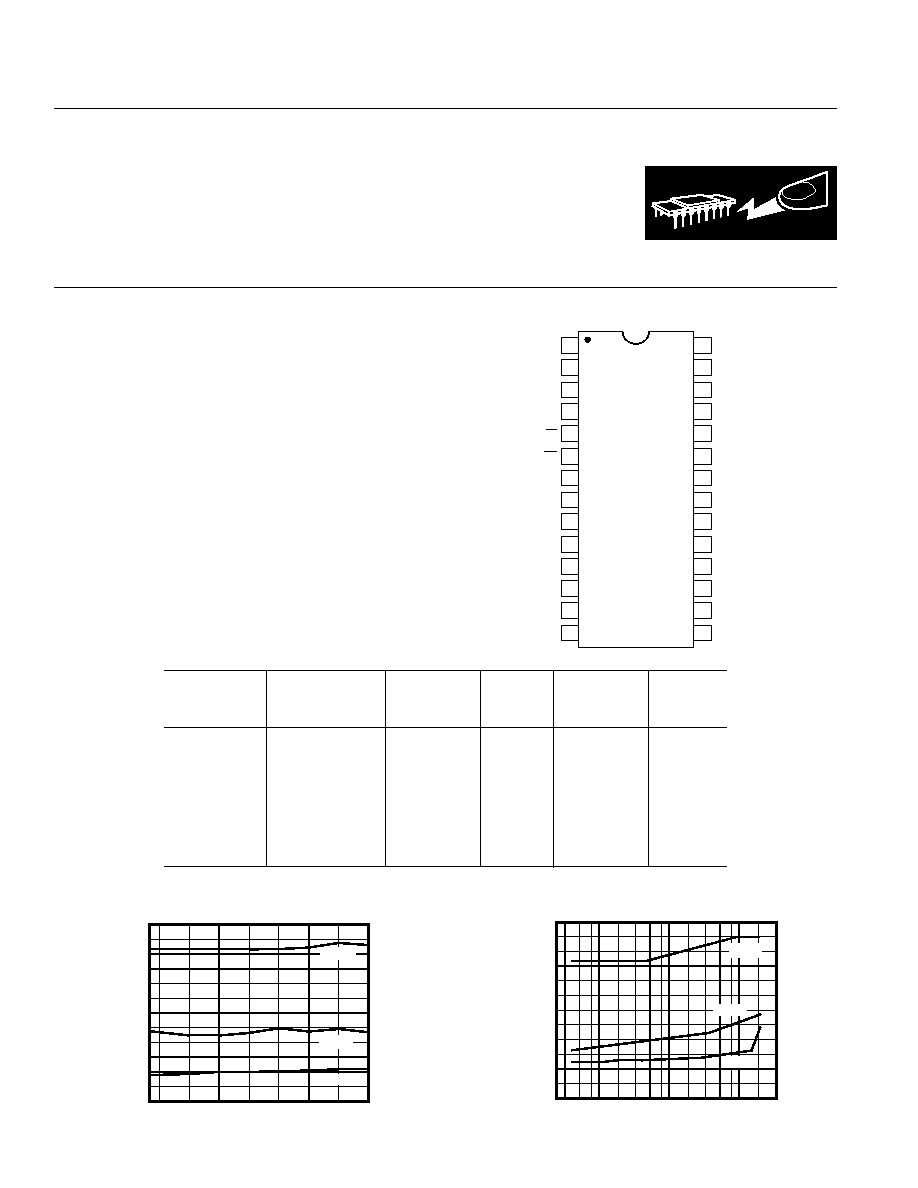
PIN CONFIGURATION
DB15
DB14
DB13
DB12
DB11
DB10
DB9
DB8
DGND
V
EE
V
CC
V
LL
CS
L1
1
2
3
4
5
6
7
8
9
10
11
12
13
14
28
27
26
25
24
23
22
21
20
19
18
17
16
15
TOP VIEW
(Not to Scale)
DB7
DB6
DB5
DB4
DB3
DB2
AGND
LDAC
DB0
DB1
AD669
REF OUT
REF IN
VOUT
SPAN/BIP
OFFSET
THD
+
N
–
%
TEMPERATURE –
°C
10
0.001
125
0.01
–25
–50
0.1
1
100
75
50
25
0
–60dB
–20dB
0dB
THD+N vs. Temperature
FREQUENCY – Hz
THD
+
N
–
%
10
0.001
0.01
0.1
1
100
10000
1000
–60dB
–20dB
0dB
THD+N vs. Frequency
相关PDF资料 |
PDF描述 |
|---|---|
| VE-B5M-MU | CONVERTER MOD DC/DC 10V 200W |
| NE592D8R2G | IC AMP VIDEO 2STAGE DIFF 8-SOIC |
| MAX4393EUB+T | IC OP AMP 85MHZ R-R 10-UMAX |
| MAX9505ETE+T | IC VIDEO AMP W/FILTER 16-TQFN |
| LTC1597-1ACG | IC D/A CONV 16BIT PAR 28-SSOP |
相关代理商/技术参数 |
参数描述 |
|---|---|
| AD669SQ | 功能描述:数模转换器- DAC IC MONO 16-BIT RoHS:否 制造商:Analog Devices 转换器数量:4 DAC 输出端数量:4 转换速率: 分辨率:12 bit 接口类型:Serial (I2C) 稳定时间: 最大工作温度:+ 105 C 安装风格: 封装 / 箱体:TSSOP 封装:Reel |
| AD669SQ/883B | 功能描述:数模转换器- DAC IC MONO 16-BIT RoHS:否 制造商:Analog Devices 转换器数量:4 DAC 输出端数量:4 转换速率: 分辨率:12 bit 接口类型:Serial (I2C) 稳定时间: 最大工作温度:+ 105 C 安装风格: 封装 / 箱体:TSSOP 封装:Reel |
| AD66BS | 制造商:POP 功能描述: 制造商:RIVETS 功能描述: |
| AD67 | 制造商:MQP (ELECTRONICS) 功能描述:ADAPTOR DIL 28WAY 制造商:MQP (ELECTRONICS) 功能描述:ADAPTOR, DIL, 28WAY 制造商:MQP (ELECTRONICS) 功能描述:ADAPTOR, DIL, 28WAY; Connector Type:Adaptor; No. of Contacts:28; Row Pitch:0.6"; Contact Termination:Through Hole Vertical; SVHC:No SVHC (19-Dec-2012); Connector Mounting Orientation:PC Board; No. of Ways:28; Package / Case:DIL; Pin ;RoHS Compliant: Yes |
| AD67 | 制造商:MQP (ELECTRONICS) 功能描述:ADAPTOR DIL 28 WAY |
发布紧急采购,3分钟左右您将得到回复。