参数资料
| 型号: | AD669BRZ-REEL |
| 厂商: | Analog Devices Inc |
| 文件页数: | 9/12页 |
| 文件大小: | 0K |
| 描述: | IC DAC 16BIT MONO VREF 28-SOIC |
| 产品变化通告: | AD669 Improvement Change 11/Jul/2012 |
| 标准包装: | 1 |
| 系列: | DACPORT® |
| 设置时间: | 10µs |
| 位数: | 16 |
| 数据接口: | 并联 |
| 转换器数目: | 1 |
| 电压电源: | 双 ± |
| 功率耗散(最大): | 625mW |
| 工作温度: | -40°C ~ 85°C |
| 安装类型: | 表面贴装 |
| 封装/外壳: | 28-SOIC(0.295",7.50mm 宽) |
| 供应商设备封装: | 28-SOIC W |
| 包装: | 标准包装 |
| 输出数目和类型: | * |
| 采样率(每秒): | 167k |
| 其它名称: | AD669BRZ-REELDKR |
AD669
REV. A
–6–
If it is desired to adjust the gain and offset errors to zero, this
can be accomplished using the circuit shown in Figure 3b. The
adjustment procedure is as follows:
STEP1 . . . ZERO ADJUST
Turn all bits OFF and adjust zero trimmer, R4, until the output
reads 0.000000 volts (1 LSB = 153
V).
STEP 2 . . . GAIN ADJUST
Turn all bits ON and adjust gain trimmer, R1, until the output
is 9.999847 volts. (Full scale is adjusted to 1 LSB less than the
nominal full scale of 10.000000 volts).
OUTPUT
GND
LDAC
DB15
(MSB)
(LSB)
DB0
CS
L1
16-BIT LATCH
10k
AMP
AD669
22
7
6
5
23
27
28
10V REF
2
1
4
3
10k
10.05k
16-BIT LATCH
16-BIT DAC
26
25
24
R2
50
R3
16k
R4
10k
+15V
–15V
R1
100
–V
EE
+V
CC
+V
LL
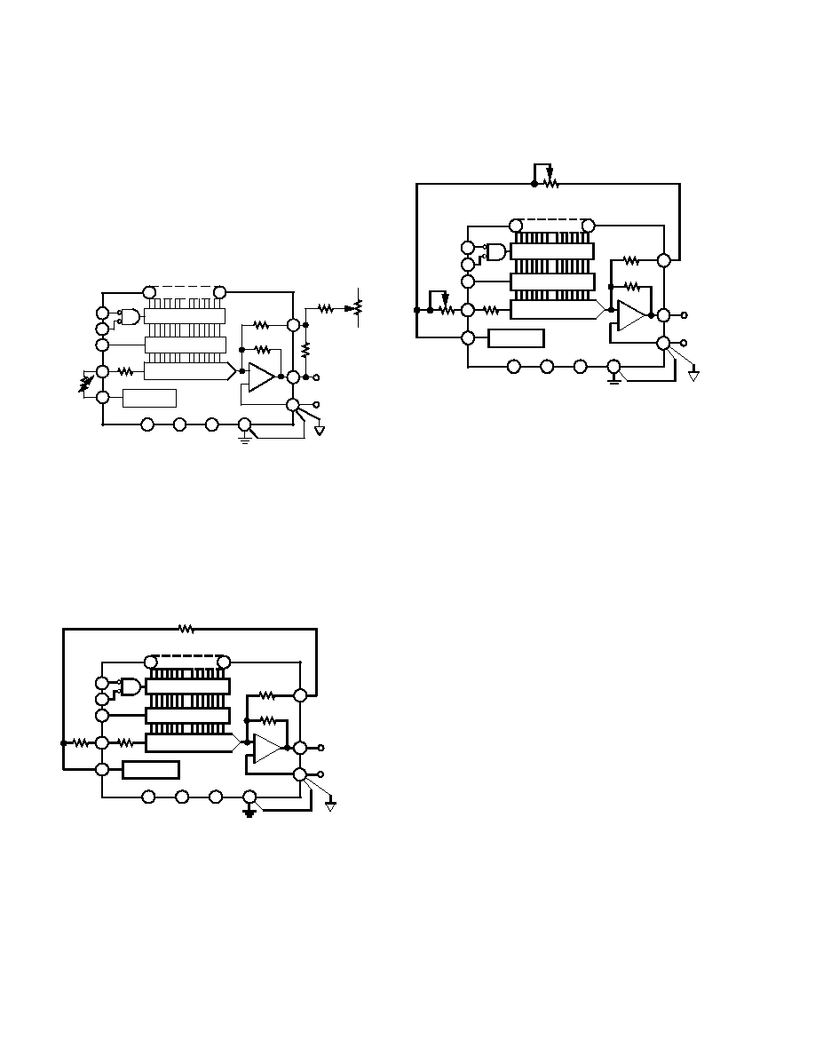
Figure 3b. 0 V to +10 V Unipolar Voltage Output with
Gain and Offset Adjustment
BIPOLAR CONFIGURATION
The circuit shown in Figure 4a will provide a bipolar output
voltage from –10.000000 V to +9.999694 V with positive full
scale occurring with all bits ON. As in the unipolar mode, resis-
tors R1 and R2 may be eliminated altogether to provide AD669
bipolar operation without any external components. Eliminating
these resistors will increase the gain error by 0.50% of FSR in
the bipolar mode.
R1
50
OUTPUT
GND
LDAC
DB15
(MSB)
(LSB)
DB0
CS
L1
16-BIT LATCH
10k
AMP
AD669
22
7
6
5
23
27
10V REF
2
14
3
26
24
10k
10.05k
16-BIT LATCH
16-BIT DAC
25
28
R2
50
–VEE
+VCC
+VLL
Figure 4a.
±10 V Bipolar Voltage Output
Gain offset and bipolar zero errors can be adjusted to zero using
the circuit shown in Figure 4b as follows:
STEP I . . . OFFSET ADJUST
Turn OFF all bits. Adjust trimmer R2 to give –10.000000 volts
output.
STEP II . . . GAIN ADJUST
Turn all bits ON and adjust R1 to give a reading of +9.999694
volts.
STEP III . . . BIPOLAR ZERO ADJUST
(Optional) In applications where an accurate zero output is re-
quired, set the MSB ON, all other bits OFF, and readjust R2
for zero volts output.
100
R1
OUTPUT
GND
LDAC
DB15
(MSB)
(LSB)
DB0
CS
L1
16-BIT LATCH
10k
AMP
AD669
22
7
6
5
23
27
10V REF
2
1
4
3
26
24
10k
10.05k
16-BIT LATCH
16-BIT DAC
25
28
100
R2
–VEE
+VCC
+VLL
Figure 4b.
±10 V Bipolar Voltage Output with Gain and
Offset Adjustment
It should be noted that using external resistors will introduce a
small temperature drift component beyond that inherent in the
AD669. The internal resistors are trimmed to ratio-match and
temperature-track other resistors on chip, even though their ab-
solute tolerances are
±20% and absolute temperature coeffi-
cients are approximately –50 ppm/
°C. In the case that external
resistors are used, the temperature coefficient mismatch be-
tween internal and external resistors, multiplied by the sensitiv-
ity of the circuit to variations in the external resistor value, will
be the resultant additional temperature drift.
INTERNAL/EXTERNAL REFERENCE USE
The AD669 has an internal low noise buried Zener diode refer-
ence which is trimmed for absolute accuracy and temperature
coefficient. This reference is buffered and optimized for use in a
high speed DAC and will give long-term stability equal or supe-
rior to the best discrete Zener diode references. The perfor-
mance of the AD669 is specified with the internal reference
driving the DAC since all trimming and testing (especially for
gain and bipolar offset) is done in this configuration.
The internal reference has sufficient buffering to drive external
circuitry in addition to the reference currents required for the
DAC (typically 1 mA to REF IN and 1 mA to BIPOLAR OFF-
SET). A minimum of 2 mA is available for driving external
loads. The AD669 reference output should be buffered with an
external op amp if it is required to supply more than 4 mA total
current. The reference is tested and guaranteed to
±0.2% max
error. The temperature coefficient is comparable to that of the
gain TC for a particular grade.
If an external reference is used (10.000 V, for example), addi-
tional trim range should be provided, since the internal refer-
ence has a tolerance of
±20 mV, and the AD669 gain and
bipolar offset are both trimmed with the internal reference. The
optional gain and offset trim resistors in Figures 5 and 6 provide
enough adjustment range to null these errors.
It is also possible to use external references other than 10 volts
with slightly degraded linearity specifications. The recom-
mended range of reference voltages is +5 V to +10.24 V, which
相关PDF资料 |
PDF描述 |
|---|---|
| VE-B5M-MU | CONVERTER MOD DC/DC 10V 200W |
| NE592D8R2G | IC AMP VIDEO 2STAGE DIFF 8-SOIC |
| MAX4393EUB+T | IC OP AMP 85MHZ R-R 10-UMAX |
| MAX9505ETE+T | IC VIDEO AMP W/FILTER 16-TQFN |
| LTC1597-1ACG | IC D/A CONV 16BIT PAR 28-SSOP |
相关代理商/技术参数 |
参数描述 |
|---|---|
| AD669SQ | 功能描述:数模转换器- DAC IC MONO 16-BIT RoHS:否 制造商:Analog Devices 转换器数量:4 DAC 输出端数量:4 转换速率: 分辨率:12 bit 接口类型:Serial (I2C) 稳定时间: 最大工作温度:+ 105 C 安装风格: 封装 / 箱体:TSSOP 封装:Reel |
| AD669SQ/883B | 功能描述:数模转换器- DAC IC MONO 16-BIT RoHS:否 制造商:Analog Devices 转换器数量:4 DAC 输出端数量:4 转换速率: 分辨率:12 bit 接口类型:Serial (I2C) 稳定时间: 最大工作温度:+ 105 C 安装风格: 封装 / 箱体:TSSOP 封装:Reel |
| AD66BS | 制造商:POP 功能描述: 制造商:RIVETS 功能描述: |
| AD67 | 制造商:MQP (ELECTRONICS) 功能描述:ADAPTOR DIL 28WAY 制造商:MQP (ELECTRONICS) 功能描述:ADAPTOR, DIL, 28WAY 制造商:MQP (ELECTRONICS) 功能描述:ADAPTOR, DIL, 28WAY; Connector Type:Adaptor; No. of Contacts:28; Row Pitch:0.6"; Contact Termination:Through Hole Vertical; SVHC:No SVHC (19-Dec-2012); Connector Mounting Orientation:PC Board; No. of Ways:28; Package / Case:DIL; Pin ;RoHS Compliant: Yes |
| AD67 | 制造商:MQP (ELECTRONICS) 功能描述:ADAPTOR DIL 28 WAY |
发布紧急采购,3分钟左右您将得到回复。